Embedding magnetic material in a cored or coreless semiconductor package

Active Publication Date: 2019-11-21
INTEL CORP
View PDF0 Cites 3 Cited by
  • Summary
  • Abstract
  • Description
  • Claims
  • Application Information

AI Technical Summary

Benefits of technology

The patent text describes a problem in semiconductor packaging where discrete inductors are expensive and require complicated embedding processes, while ACIs (air core inductors) have lower magnetic permeability and may not generate inductance as effectively as discrete inductors. The text proposes a solution by fabricating an ACI comprising a magnetic material to increase its magnetic permeability and enhance its performance. However, magnetic materials are not easily integrated into current semiconductor fabrication processes and may cause difficulties in laser drilling of vias and contamination of bath chemistries and tools used in etching techniques.

Problems solved by technology

There are some drawbacks associated with discrete inductors.
Discrete inductors can be costly (when compared to ACIs).
Also, the embedding processes used to incorporate discrete packages into semiconductor packages can be complicated.
Additionally, the surface mounting processes used to incorporate discrete packages into semiconductor packages can add an undesired thickness (e.g., z-height, etc.) to the overall thickness of the resulting semiconductor package.
Discrete inductors might also require extra space outside a semiconductor package, which can be difficult to achieve in high-density microelectronic devices.
Additionally, because discrete inductors are usually prepackaged devices that are proprietary to third party vendors, package design may be limited.
ACIs have some drawbacks even though they can be less expensive than discrete inductors.
One drawback is that ACIs may not generate inductance as effectively or as efficiently as discrete inductors.
Another drawback is that ACIs can take up valuable real estate in a package substrate in order to generate a target inductance, which can in turn reduce the achievable input / output (I / O) density per mm per layer (IO / mm / layer) in a semiconductor package.
Magnetic materials, however, are not easily integrated into current semiconductor fabrication processes that comply with current industry standards.
One drawback associated with the magnetic material(s) is that laser drilling of vias through the magnetic material(s) may be difficult, costly, or complicated.
For a first example, after laser drilling of a magnetic material to form vias is performed, some of the material's magnetic fillers are not ablated away, which in turn leaves residue in the resulting vias creating unwanted “dirty vias.” Another drawback associated with the magnetic material(s) is a risk of contamination of bath chemistries associated with wet processes and / or a risk of contamination of tools or materials used in etching techniques.
For example, magnetic fillers in the magnetic material(s) may have negative, undesirable, or unexpected interactions with bath chemistries, materials, and / or tools used in, for example, desmearing processes, electroless plating processes, flash etching processes, soft etching processes, seed etching processes, processes involving roughening baths.
For another example, introduction of magnetic material(s) to certain bath chemistries may result in corrosion, destruction, dissolution, or degradation of the magnetic fillers in the magnetic material(s).
For this example, corrosion of the magnetic fillers may cause the magnetic fillers to leach into bath chemistries, which can in turn contaminate the baths and reduce the life cycle of the baths.
These tailoring processes, however, can be time-consuming and expensive endeavors, which can in turn increase costs associated with semiconductor manufacturing and / or packaging.
Furthermore, these tailoring processes may run a risk of over-engineering—that is, the magnetic material(s), the bath chemistries associated with wet processes, and / or the tools or materials used in etching techniques may be suboptimally designed.

Method used


Image

  • Embedding magnetic material in a cored or coreless semiconductor package
  • Embedding magnetic material in a cored or coreless semiconductor package
  • Embedding magnetic material in a cored or coreless semiconductor package

Examples


Embodiment Construction

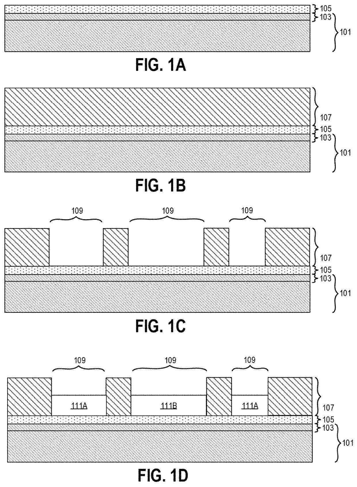
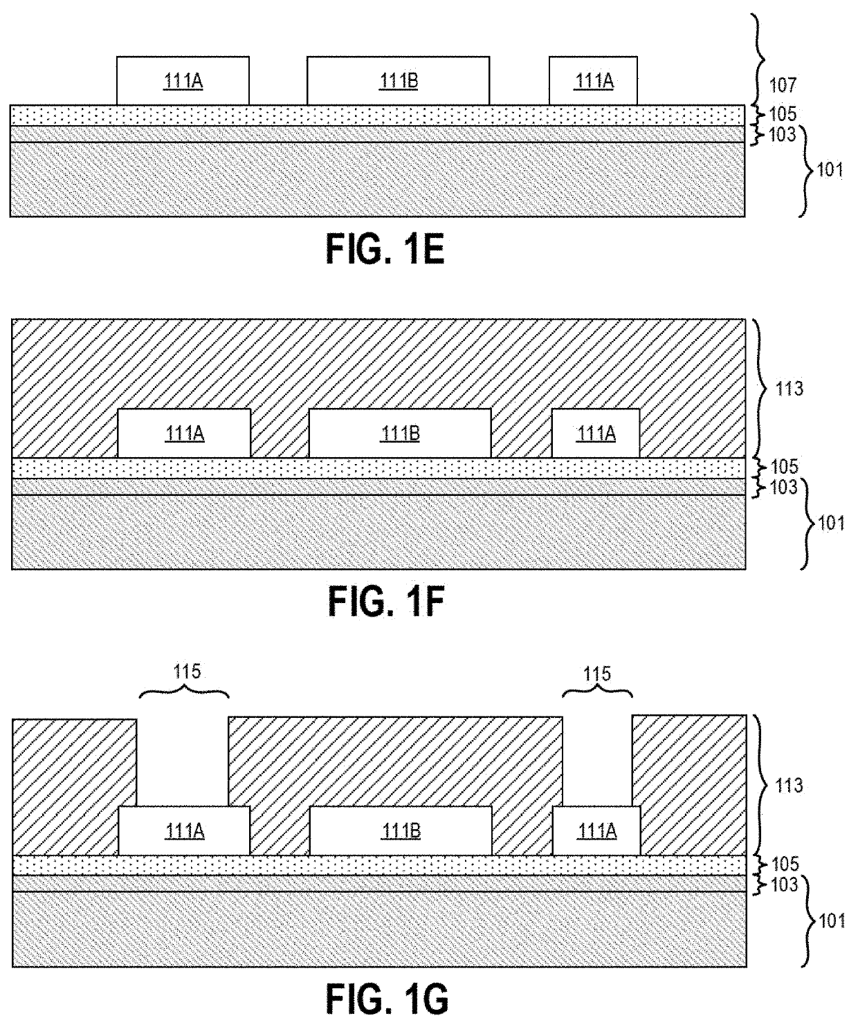
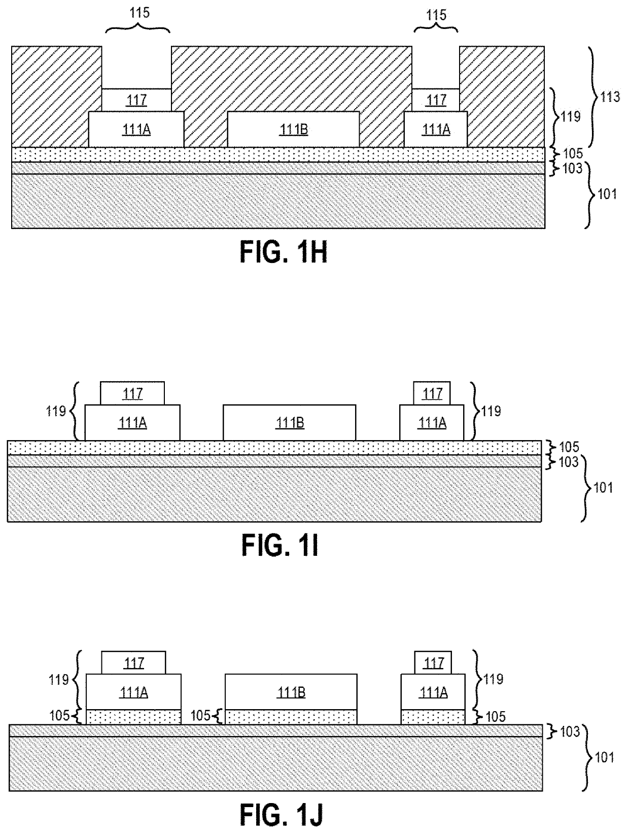
[0015]Embodiments described herein provide techniques that can assist with fabricating a cored or coreless semiconductor package having one or more magnetic materials embedded therein. For one or more embodiments, an inductor in a cored or coreless semiconductor package comprises one or more of the magnetic materials. Several advantages are provided by the embodiments described herein. One advantage is that the embodiment(s) described herein can assist with creating a chemically resilient technique of manufacturing an inductor comprising one or more of the embedded magnetic materials in a cored or coreless semiconductor package. Another advantage is that the embodiment(s) described herein can assist with providing flexibility towards the choice of materials used for fabricating a cored or coreless semiconductor package. Yet another advantage is that magnetic material(s), which are embedded in a semiconductor package that is fabricated in accordance with one or more of the embodiment...


PUM


Abstract

Techniques for fabricating a semiconductor package having magnetic materials embedded therein are described. For one technique, fabrication of package includes: forming a pad and a conductive line on a build-up layer; forming a raised pad structure on the build-up layer, the raised pad comprising a pillar structure on the pad; encapsulating the conductive line and the raised pad structure in a magnetic film comprising one or more magnetic fillers; planarizing a top surface of the magnetic film until top surfaces of the raised pad structure and the magnetic film are co-planar; depositing a primer layer on the top surfaces; removing one or more portions of the primer layer above the raised pad structure to create an opening; and forming a via in the opening on the raised pad structure. The primer layer may comprise one or more of a build-up layer, a photoimageable dielectric layer, and a metal mask.

Description

BACKGROUNDField[0001]Embodiments described herein relate to semiconductor packages. More specifically, the described embodiments are directed to semiconductor packages having one or more magnetic materials embedded therein and techniques of forming such packages.Background Information[0002]An inductor is a passive electronic component that is typically included in a semiconductor package comprising one or more semiconductor dies. One or more inductors can be used to form a functional or fully integrated voltage regulator (IVR). The IVR can provide one or more voltage regulators for semiconductor die(s) within a semiconductor package.[0003]Inductors used in semiconductor packages can take multiple forms. Examples include, but are not be limited to, discrete inductors and air core inductors (ACIs).[0004]Discrete inductors are generally prepackaged inductor devices (e.g., off-chip, off-package devices comprising one or more inductors, etc.). Discrete inductors typically include at leas...

Claims


Application Information

Patent Timeline
IPC IPC(8): H01L23/64H01L23/498H01L21/48H01L23/00H01F1/12H01F41/14
CPCH01L2924/19103H01L23/49838H01L21/4857H01L23/49866H01F1/12H01L24/16H01L21/4867H01L2224/16225H01L23/645H01L2924/19042H01F41/14H01L23/49822H01F41/16H01F1/0027H01L25/16H01L2224/16227
Inventor LEE, KYU-OHVADLAMANI, SAIJAIN, RAHULZHAO, JUNNANPARK, JI YONGXU, CHENGKIM, SEO YOUNG
Owner INTEL CORP
Why Eureka
Try Eureka