Apparatus, and process for cold spray deposition of thermoelectric semiconductor and other polycrystalline materials and method for making polycrystalline materials for cold spray deposition

a technology of thermoelectric semiconductor and other polycrystalline materials, applied in the direction of thermoelectric device junction materials, thermoelectric device manufacturing/treatment, pressure inorganic powder coating, etc., can solve the problems of difficult integration into waste heat sources, waste heat, and little attention, and achieve the effect of enhancing the cold spray deposition of thermoelectric semiconductors and enhancing the cold spray deposition of crystalline materials

Active Publication Date: 2019-11-21
THUSS RICHARD C
View PDF0 Cites 2 Cited by
  • Summary
  • Abstract
  • Description
  • Claims
  • Application Information

AI Technical Summary

Benefits of technology

[0007]Using a supersonic cold-spray process, the adhesion to the surface and deposition of near theoretical density layers of both N-type and P-type thermoelectric semiconductor materials and other polycrystalline particles has been achieved by controlling the shapes of the particles in the thermoelectric semiconductor powder material, the maximum particle size and the particle size distribution, incorporating a powder flow and deposition enhancing additive materials, utilizing specifically configured cold spray nozzle and preheated pressurized gas process, and controlling the thermoelectric semiconductor peak particle velocities. Thermoelectric semiconductor powder materials, equipment design, and process parameters have been developed to enable and enhance the cold-spray deposition of thermoelectric semiconductor and other crystalline materials onto metals, glass, ceramic, and high temperature capable polymer surfaces. The powder used in the supersonic cold spray process is controlled to volumetrically have greater than 95% of the particles with a maximum particle size not greater than 15 micrometers and a controlled volumetric particle size distribution over the nominal particle size ranges, from 0.1-6.0 micrometers; 2.0-10.0 micrometers; and 5.0-15 micrometers in major dimension, and by the incorporation of powder flow and deposition enhancing additive materials, such as, but not limited to, hollow glass microspheres, when combined with 1.0-2.0 mm diameter cold spray nozzle throat dimensions, a nozzle throat area to exit area expansion ratios of 6-10, a nozzle divergent / convergent length ratios between 1 and 3, a nitrogen gas process parameters of 450-550 degrees centigrade pre-heat, and gas pressures from 0.4-0.9 million pascal (MPa) yielding gas and particle velocities from 750 to 900 meters / second, an adhesion to the surface and deposition of near theoretical density layers of both N-type and P-type thermoelectric semiconductor materials and other poly crystalline particles has been achieved. Using this process, the semiconductor materials are deposited onto flat as well as complex shaped surfaces in both thin and thick layers, and from individual small pellet sized spots to large continuous areas, thus enabling TEG designs specifically tailored to the application and the heat source. Supersonic cold-spray deposition of thermoelectric materials such as bismuth telluride, antimony telluride, and Tetrahedrite type copper sulfosalts have been demonstrated, and these processes can also apply to functional materials used in other solid state energy harvesting techniques, such as but not limited to piezoelectric devices, thermopiles, as well as for thermoelectric cooling (TECs) devices. Unique powder material composition, particle shape and sizes, and control of the cold-spray process parameters and equipment design allow the uniform cold spray deposition to a surface of polycrystalline materials such as thermoelectric semiconductor materials, and the developed process further enables and enhances the cold spray deposition of crystalline and other non-malleable particles of irregular shapes and dimensions of less than 10 micrometers.

Problems solved by technology

Waste heat is a significant global environmental issue, but it is one that draws little attention because of very limited solutions.
Thermoelectric generators or (TEGs) using solid state conversion of heat to electricity is one technology for application to waste heat recovery, but TEGs are currently only used in niche markets because the resulting cost per kilowatt is high, and they are difficult to integrate into waste heat sources because of their flat plate form factor.
As recognized by the present inventor, the flat form factor makes the TEGs difficult to thermally couple to complex shaped heat sources and equally difficult to couple to active cooling sources, both issues adding significantly to TEG installation complexity and cost.
The present inventor also recognized that TEGs made using semi-conductor pellets also require the use of solders to hold the multilayer thermoelectric couple element assembly together, and these materials often limit potential applications and the maximum electrical output of the devices.
The overall design of current commercial thermoelectric devices also make them subject to degradation or failure when subjected to moderate to intense mechanical and thermal shock environments.
One potential method of achieving both the deposition of the thermoelectric semiconductor and metallic materials is the use of the supersonic cold-spray deposition process, although the industry has struggled to find a solution that achieves that objective.

Method used


Image

  • Apparatus, and process for cold spray deposition of thermoelectric semiconductor and other polycrystalline materials and method for making polycrystalline materials for cold spray deposition
  • Apparatus, and process for cold spray deposition of thermoelectric semiconductor and other polycrystalline materials and method for making polycrystalline materials for cold spray deposition
  • Apparatus, and process for cold spray deposition of thermoelectric semiconductor and other polycrystalline materials and method for making polycrystalline materials for cold spray deposition

Examples


Embodiment Construction

[0024]Supersonic cold spray process can be used extensively for the deposition of metallic materials including aluminum, copper, nickel, and many others metals and their alloys.

The process can be used for a variety of applications including metals repair, corrosion control, and the application of hardened surface coatings. Optimization of the final deposited material is achieved by the selection of numerous powder material, equipment, and supersonic cold-spray process parameters.

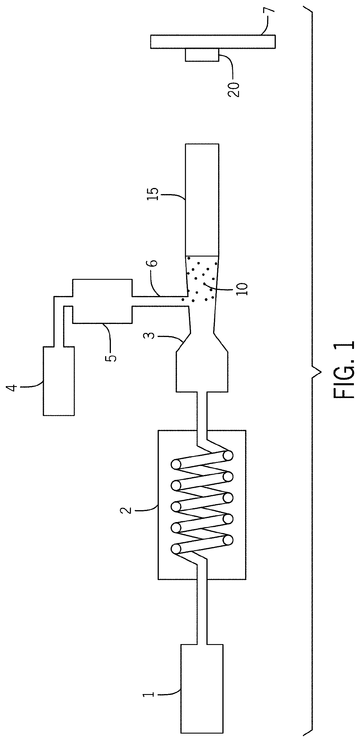
[0025]FIG. 1 is a high-level diagram of one type of equipment currently used for the cold spray deposition of metallic materials. A gas 1 such as, air, nitrogen or helium is pressurized in the range of from 0.5-3.5 MPa. This pressurized gas 1 is directed into a heater 2 and is heated to 300-550 degrees centigrade. This gas is then directed through a converging-diverging nozzle 3 with a throat diameter between 2.0 millimeter and 2.5 millimeter where the gas 1 is accelerated to supersonic velocity. In this exi...


PUM

PropertyMeasurementUnit
particle diameteraaaaaaaaaa
pressureaaaaaaaaaa

Abstract

An apparatus and method perform supersonic cold-spraying to deposit N and P-type thermoelectric semiconductor, and other polycrystalline materials on other materials of varying complex shapes. The process developed has been demonstrated for bismuth and antimony telluride formulations as well as Tetrahedrite type copper sulfosalt materials. Both thick and thin layer thermoelectric semiconductor material is deposited over small or large areas to flat and highly complex shaped surfaces and will therefore help create a far greater application set for thermoelectric generator (TEG) systems. This process when combined with other manufacturing processes allows the total additive manufacturing of complete thermoelectric generator based waste heat recovery systems. The processes also directly apply to both thermoelectric cooler (TEC) systems, thermopile devices, and other polycrystalline functional material applications.

Description

[0001]This present application claims the benefit of the earlier filing date of U.S. Provisional patent application, Ser. No. 62 / 673,556 filed 18 May 2018, the entire contents of which being incorporated by reference herein in its entirety.[0002]The present application also contains subject matter related to that in U.S. Pat. No. 9,306,146, the entire contents of which is incorporated herein by reference.BACKGROUND[0003]Waste heat is a significant global environmental issue, but it is one that draws little attention because of very limited solutions. A large fraction of energy used in industrial processes and transportation systems is lost as low grade waste heat, and several trillion dollars of energy generated from fossil fuels in the U.S. each year, equal to nearly sixty quadrillion BTUs, is discarded without benefit in the form of waste heat.[0004]Thermoelectric generators or (TEGs) using solid state conversion of heat to electricity is one technology for application to waste he...

Claims


Application Information

Patent Timeline
Patent Type & Authority Applications(United States)
IPC IPC(8): H01L35/34H01L35/16H01L35/14H01L35/28C23C24/04
CPCH01L35/34H01L35/16H01L35/28H01L35/14C23C24/04B05B7/205H10N10/851H10N10/10H10N10/852H10N10/01
Inventor THUSS, RICHARD C
Owner THUSS RICHARD C
Why Eureka
Try Eureka