Charge transporting varnish and charge transporting thin film using the same
a charge transporting film and charge technology, applied in the direction of electroluminescent light sources, coatings, electric conductive paints, etc., can solve the problems of color purity and color reproducibility of organic el devices, color film, color purity, etc., to improve other characteristics, reduce the coloration of charge transporting films, and improve light transmittance
- Summary
- Abstract
- Description
- Claims
- Application Information
AI Technical Summary
Benefits of technology
Problems solved by technology
Method used
Image
Examples
example 1-1
[0229]First, under a nitrogen atmosphere, 0.060 g of the aniline derivative represented by formula (A1) synthesized according to the method described in WO 2013 / 084664 and 0.120 g of the arylsulfonic acid represented by formula (S1) synthesized according to the method described in WO 2006 / 025342 were dissolved in 5.8 g of 1,3-dimethyl-2-imidazolidinone. To this was added 7.8 g of 2,3-butanediol and 4.2 g of dipropylene glycol monomethyl ether, followed by stirring, after which 2.029 g of a silica sol dispersed in ethylene glycol (EG-ST, manufactured by Nissan Chemical Industries, Ltd., particle size: 10 nm-15 nm, SiO2: 20.5 wt. %) was added and stirred to obtain a varnish for forming a hole injection layer.
example 2-1
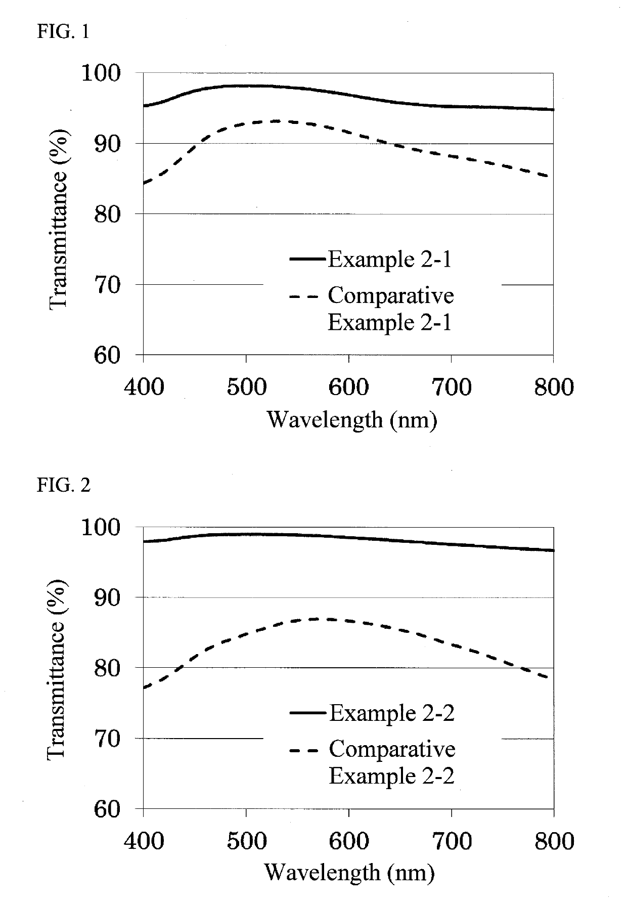
[0231]The varnish obtained in Example 1-1 was applied to a quartz substrate using a spin coater, and then dried by baking in an air atmosphere at 80° C. for 1 minute. Next, the dried quartz substrate was baked at 230° C. for 15 minutes in an air atmosphere to form a uniform film of 50 nm thickness on the quartz substrate.
example 3-1
[0235]The varnish obtained in Example 1-1 was applied to an ITO substrate using a spin coater, and was subsequently dried at 80° C. under air atmosphere for 1 minute. Subsequently, the dried substrate was baked at 230° C. for 15 minutes under air atmosphere to form a uniform film, 50 nm thick, on the ITO substrates. For the ITO substrate, a glass substrate (25 mm×25 mm×0.7 t) on the surface of which a patterned indium tin oxide (ITO) film having a thickness of 150 nm was formed was used, and the impurities on the surface of the glass substrate were removed by an O2 plasma cleaning device (150 W, 30 seconds) prior to use.
[0236]Next, α-NPD (N,N′-di(1-naphthyl)-N,N′-diphenylbenzidine) was deposited using an vacuum evaporator (degree of vacuum: 1.0×10⁻⁵ Pa) to a thickness of 120 nm at a rate of 0.2 nm / sec on the ITO substrate on which the film was formed. Next, another film of HTEB-01 (an electron blocking material manufactured by Kanto Chemical Co., Ltd.) was formed having a thickness ...
PUM
| Property | Measurement | Unit |
|---|---|---|
| Mass | aaaaa | aaaaa |
| Wavelength | aaaaa | aaaaa |
| Wavelength | aaaaa | aaaaa |
Abstract
Description
Claims
Application Information


