Method for manufacturing wafer

a manufacturing method and wafer technology, applied in the direction of manufacturing tools, lapping machines, edge grinding machines, etc., can solve the problem of reducing the flatness of the wafer by a high etching ra

Active Publication Date: 2020-01-02
SHIN-ETSU HANDOTAI CO LTD
View PDF0 Cites 1 Cited by
  • Summary
  • Abstract
  • Description
  • Claims
  • Application Information

AI Technical Summary

Benefits of technology

[0032]The inventive method for manufacturing a wafer makes it possible to manufacture a wafer product having R1 and R2 within a target value range, the wafer having a uniform chamfered cross-sectional shape in the circumferential direction in comparison with wafers manufactured by the conventional techniques. Particularly, even when the etching is performed with an alkali which is likely to affect the chamfered cross-sectional shape in the wafer circumferential direction, it is possible to manufacture a wafer having a uniform chamfered cross-sectional shape in the circumferential direction.

Problems solved by technology

The acid etching is advantageous in that the etching rate and the surface state are easily controlled, but also has such a disadvantage that its high etching rate decreases the flatness of the wafer which had been improved by the lapping and double-side grinding.

Method used


Image

  • Method for manufacturing wafer
  • Method for manufacturing wafer
  • Method for manufacturing wafer

Examples


example 1

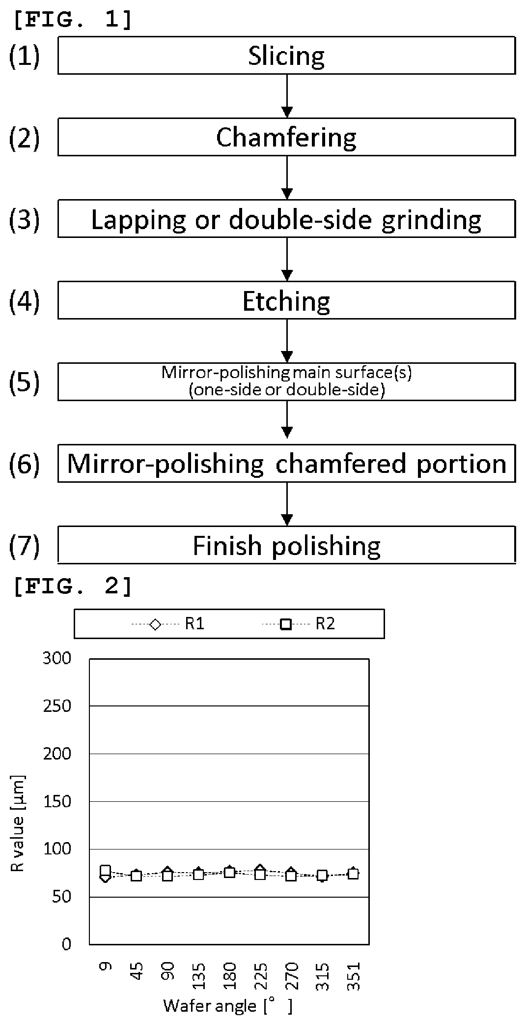
[0068]A wafer was prepared as follows while the target values of R1, R2 of the final wafer product were set to 220 μm or more and 300 μm or less.

[0069]First, a single crystal silicon ingot was sliced to obtain a sliced wafer (step 1). Next, a grinding wheel was rotated at high speed. The grinding wheel used had a groove shape designed to make the chamfered cross-sectional shape dimensions of the R1 value and the R2 value within a range of 50 μm or more and 100 μm or less. After the slicing step, a circumferential edge portion of the silicon wafer held on a holding stage was brought into contact with the grinding wheel, and chamfered by rotating the wafer (step 2).

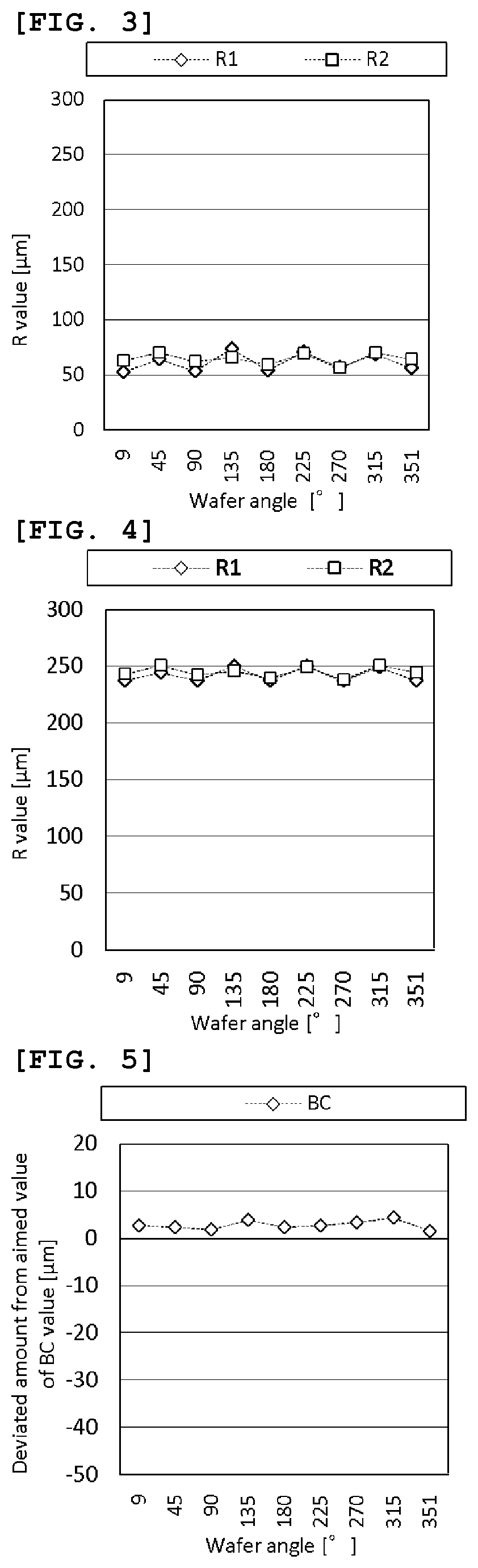
[0070]At this point (immediately after the chamfering in step 2), the chamfered cross-sectional shape dimensions of the R1 value and the R2 value were measured at nine spots inside the circumference of the silicon wafer, specifically, nine positions at intervals of 45°, including 9° and 351°, with respect to a notch. FIG. 2...

example 2

[0075]A sliced wafer was obtained by the same method as in Example 1, and then chamfered with a grinding wheel by the same method as in Example 1. The grinding wheel used had a groove shape designed to make the chamfered cross-sectional shape dimensions of the R1 value and the R2 value within 150 to 200 μm.

[0076]Next, the double-side grinding, alkali etching, double-side mirror-polishing, and chamfered-portion mirror-polishing were successively performed by the same method as in Example 1.

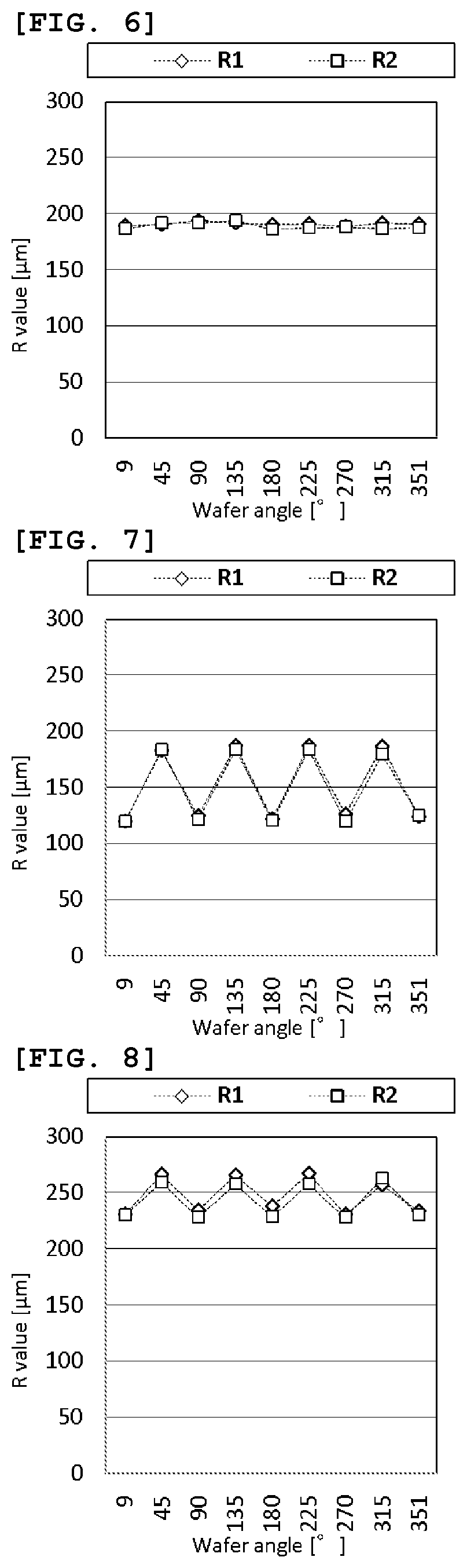
[0077]As in Example 1, after the chamfering step, after the alkali etching step, and after the chamfered-portion mirror-polishing step, the chamfered cross-sectional shape dimensions were measured at the same positions as in Example 1 and under the same conditions as the above measurement conditions. FIG. 6 shows the chamfered cross-sectional shape dimensions of the R1 value and the R2 value after the chamfering step. FIG. 7 shows the chamfered cross-sectional shape dimensions of the R1 value and t...


PUM

PropertyMeasurementUnit
thicknessaaaaaaaaaa
temperatureaaaaaaaaaa
shapeaaaaaaaaaa

Abstract

A method for manufacturing a wafer product, including the steps of: chamfering a circumferential edge portion of a wafer; lapping or double-side grinding main surfaces thereof; etching; mirror-polishing the main surface; and mirror-polishing the chamfered portion. The chamfered portion has a cross-sectional shape including: a first inclined portion continuous from the first main surface; a first arc portion continuous from the first inclined portion and having a radius of curvature; a second inclined portion continuous from the second main surface; a second arc portion continuous from the second inclined portion and having a radius of curvature; and an end portion connecting the first arc portion to the second arc portion. This provides a method for manufacturing a wafer by which a variation in a chamfered cross-sectional shape in a circumferential direction caused by etching can be suppressed.

Description

TECHNICAL FIELD[0001]The present invention relates to a method for manufacturing a wafer.BACKGROUND ART[0002]In a method for manufacturing a semiconductor wafer, the following steps are successively performed in general: (a) a slicing step for cutting a thin wafer from a single crystal ingot, (b) a chamfering step for preventing cracking of an outer circumferential portion of the wafer, (c) a lapping step or double-side grinding step for eliminating the thickness variation of the wafer, (d) an etching step for removing processing damage or contaminant introduced by the chamfering, the lapping, or the grinding, (e) a mirror-polishing step for polishing one or both of main surfaces of the wafer to a mirror finish, and (f) a mirror-polishing step for polishing the chamfered portion to a mirror finish.[0003]The etching step includes, for example, acid etching using an acid mixture containing hydrofluoric acid, nitric acid, acetic acid, and the like; and alkali etching using an alkali su...

Claims


Application Information

Patent Timeline
Patent Type & Authority Applications(United States)
IPC IPC(8): H01L21/02H01L21/304
CPCH01L21/02021H01L21/304H01L21/02024H01L21/02013B24B9/00B24B37/00H01L21/02019H01L21/02016
Inventor NAKATANI, YUYA
Owner SHIN-ETSU HANDOTAI CO LTD
Why Eureka
Try Eureka