Current pulse generator with integrated bus boost circuit

a current pulse generator and boost circuit technology, applied in the direction of electric variable regulation, process and machine control, instruments, etc., can solve the problems of severe limitations on the size of the pulse generator with conventional mosfet power transistors, and the limited switching speed of silicon-based transistors, so as to reduce the area of the current pulse generator, increase the pulse frequency, and reduce the effect of current pulse generator area

Active Publication Date: 2020-01-23
EFFICIENT POWER CONVERSION CORP
View PDF10 Cites 1 Cited by
  • Summary
  • Abstract
  • Description
  • Claims
  • Application Information

AI Technical Summary

Benefits of technology

[0009]The present invention addresses the disadvantages of conventional boost converters and current pulse generators, discussed above, by providing a boost converter circuit incorporated with gallium nitride (GaN) FET transistor switches, which may be monolithically integrated into a single semiconductor die with the corresponding gate drivers, reducing the area of the current pulse generator. The high switching speeds of the GaN FETs included in the present invention also provide a boost converter circuit with the capability to operate at an increased pulse frequency.
[0010]The present invention, as described herein, comprises a first gate driver circuit connected to a GaN FET, which controls the charging of a capacitor in a boost converter. A second gate driver circuit is connected to a second GaN FET transistor, which controls the discharging of the capacitor through a load connected to the boost converter. Both GaN FET transistors are preferably enhancement mode GaN FETs and may be integrated into a single semiconductor chip in combination with the first and second gate driver circuits. The diode in a conventional boost converter circuit can also be implemented in the present invention as a GaN FET transistor, which is also integrated into the single semiconductor chip in combination with its gate driver circuit. As a result, the entire current pulse generator circuit of the present invention can advantageously be integrated in a single semiconductor die.

Problems solved by technology

However, the switching transistors must be able to withstand the higher voltages and currents through the boost converters, which may require larger area power transistors.
This severely limits how small a pulse generator with conventional MOSFET power transistors can be made.
Similarly, more frequent, smaller, and accurate pulses enable higher frame rates and better distance resolution for the lidar system, but the switching speed of silicon-based transistors is limited.

Method used


Image

  • Current pulse generator with integrated bus boost circuit
  • Current pulse generator with integrated bus boost circuit
  • Current pulse generator with integrated bus boost circuit

Examples


Embodiment Construction

[0024]In the following detailed description, reference is made to certain embodiments. These embodiments are described with sufficient detail to enable those skilled in the art to practice them. It is to be understood that other embodiments may be employed and that various structural, logical, and electrical changes may be made. The combinations of features disclosed in the following detailed description may not be necessary to practice the teachings in the broadest sense, and are instead taught merely to describe particularly representative examples of the present teachings.

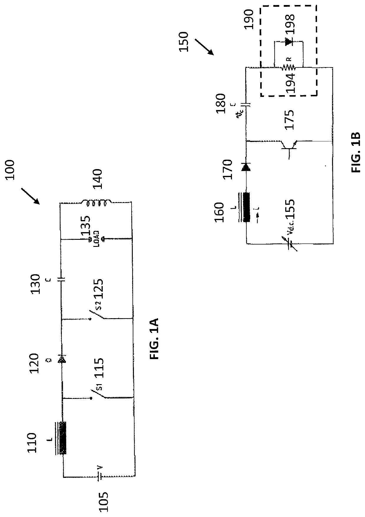
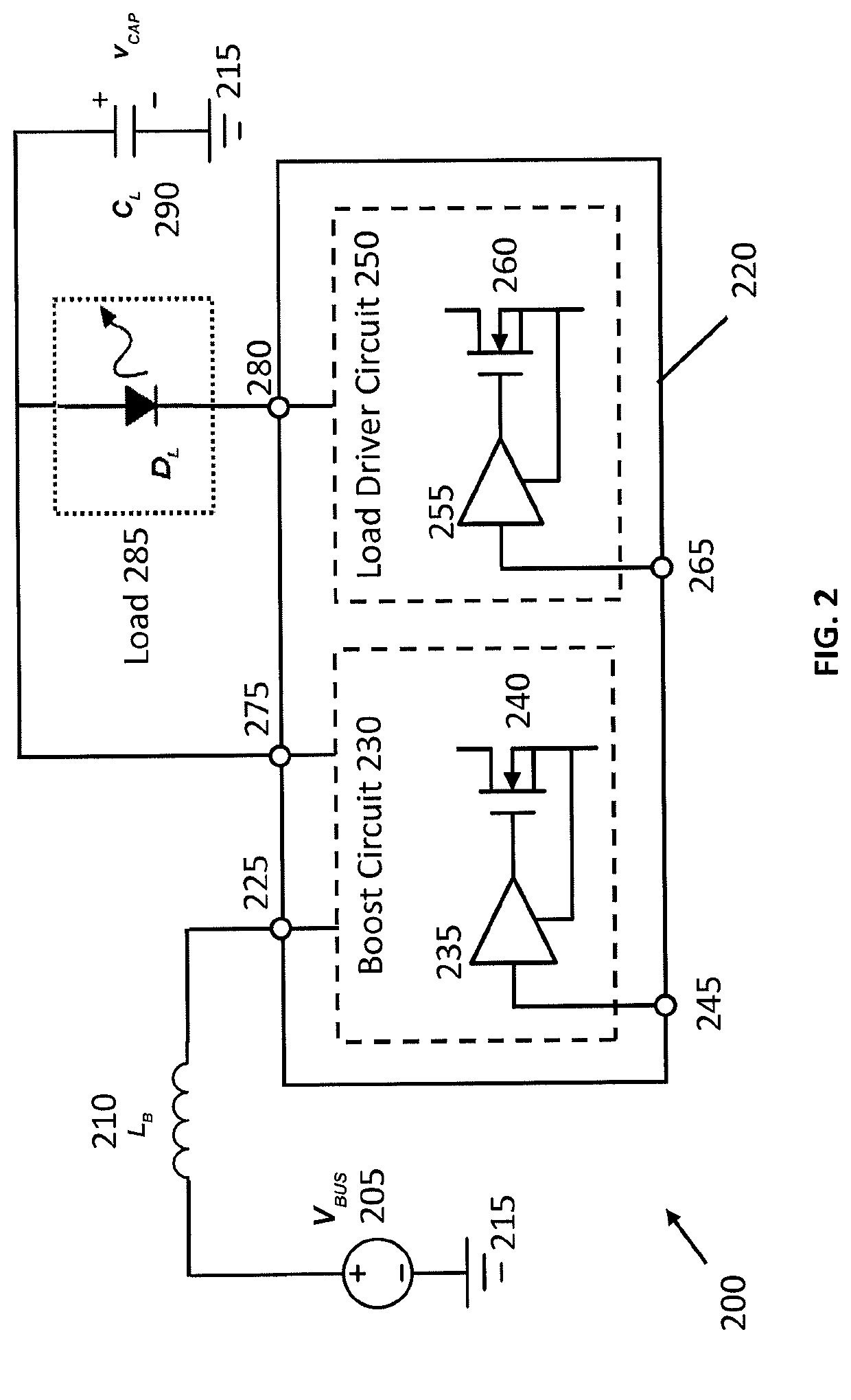
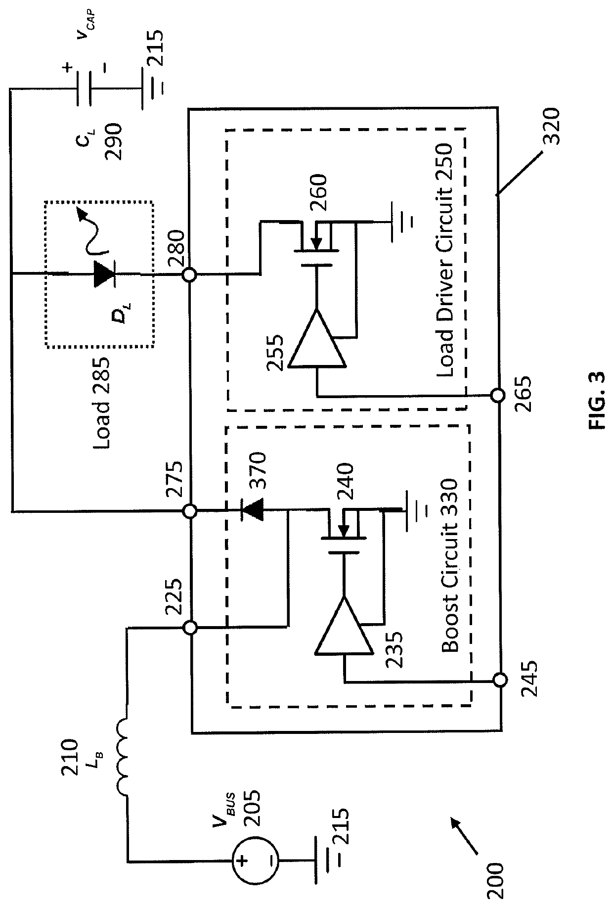
[0025]FIG. 2 illustrates a current pulse generator 200 according to an exemplary embodiment of the present invention, with GaN FET transistors integrated into a single monolithic chip 220. Monolithic integration of boost circuit 230 and load driver circuit 250 onto a single semiconductor die 220 greatly reduces the area of current pulse generator 200. Pulse generator 200 is similar to the boost converters and cu...


PUM

PropertyMeasurementUnit
pulsing frequenciesaaaaaaaaaa
electrical energyaaaaaaaaaa
impedanceaaaaaaaaaa

Abstract

A current pulse generator circuit configured to be monolithically integrated into a single semiconductor die and provide high pulsing frequencies. A first GaN FET transistor controls the charging of a capacitor in a boost converter. A second GaN FET transistor controls the discharging of the capacitor through a load, such as a laser diode, connected to the boost converter. Both GaN FET transistors are preferably enhancement mode GaN FETs and may be integrated into the single semiconductor die, together with gate drivers. The diode in a conventional boost converter circuit can also be implemented in the present invention as a GaN FET transistor, and also integrated into the single semiconductor die.

Description

[0001]This application claims the benefit of U.S. Provisional Application No. 62 / 699,990, filed on Jul. 18, 2018, the entire disclosure of which is hereby incorporated by reference.BACKGROUND1. Field of the Invention[0002]The present invention relates generally to power current pulse generators, and more particularly to a boost converter with higher pulsing frequencies and a smaller form factor.2. Description of the Related Art[0003]Typical current pulse generator circuits include a storage capacitor, a load, and a discharge device, which may be implemented with a semiconductor device such as a transistor. The storage capacitor stores electrical energy, and the discharge device controls current supplied by the capacitor to the load. The energy stored in the capacitor may be controlled or limited by impedance in the current loop formed by the capacitor, discharge device, and load. To generate high energy pulses from the capacitor to the load, the capacitor is often charged to a highe...

Claims


Application Information

Patent Timeline
Patent Type & Authority Applications(United States)
IPC IPC(8): H02M3/158H02M1/42H03K5/02
CPCH02M3/1584H03K5/02H02M2003/1586H02M1/4225H02M3/158H02M3/1588Y02B70/10H02M3/1586
Inventor GLASER, JOHN S.COLINO, STEPHEN L.
Owner EFFICIENT POWER CONVERSION CORP
Why Eureka
Try Eureka