Method for depositing oxide film by peald using nitrogen

a technology of oxide film and nitrogen, which is applied in the direction of chemical vapor deposition coating, coating, electric discharge tube, etc., can solve the problems of difficult control of patterning size in a desired range, inability to ignore the above problem in the process of next generation devices, and the adverse effect of etching of photoresis

Inactive Publication Date: 2020-04-09
ASM IP HLDG BV
View PDF3 Cites 204 Cited by
  • Summary
  • Abstract
  • Description
  • Claims
  • Application Information

AI Technical Summary

Benefits of technology

[0004]Some embodiments of the present invention provide a method of suppressing a size reduction of patterns formed with an organic material (e.g., a photoresist) while depositing an insulation film thereon by reducing adverse effect (e.g., etching the organic material) by the deposition process. Conventionally, Ar has been used as a carrier gas for feeding a precursor to a reaction chamber, and a plasma of a mixture of Ar and O2 has been used for depositing an insulation film. Some embodiments are characterized in that N2 is

Problems solved by technology

However, conventional PEALD for depositing a SiO2 film uses a plasma of a mixed gas of Ar and O2, in which a photoresist is exposed to the plasma in the beginning of deposition until the photoresist is covered by a SiO2 film, thereby causing the photoresist to be et

Method used


Image

  • Method for depositing oxide film by peald using nitrogen
  • Method for depositing oxide film by peald using nitrogen
  • Method for depositing oxide film by peald using nitrogen

Examples


reference example 1

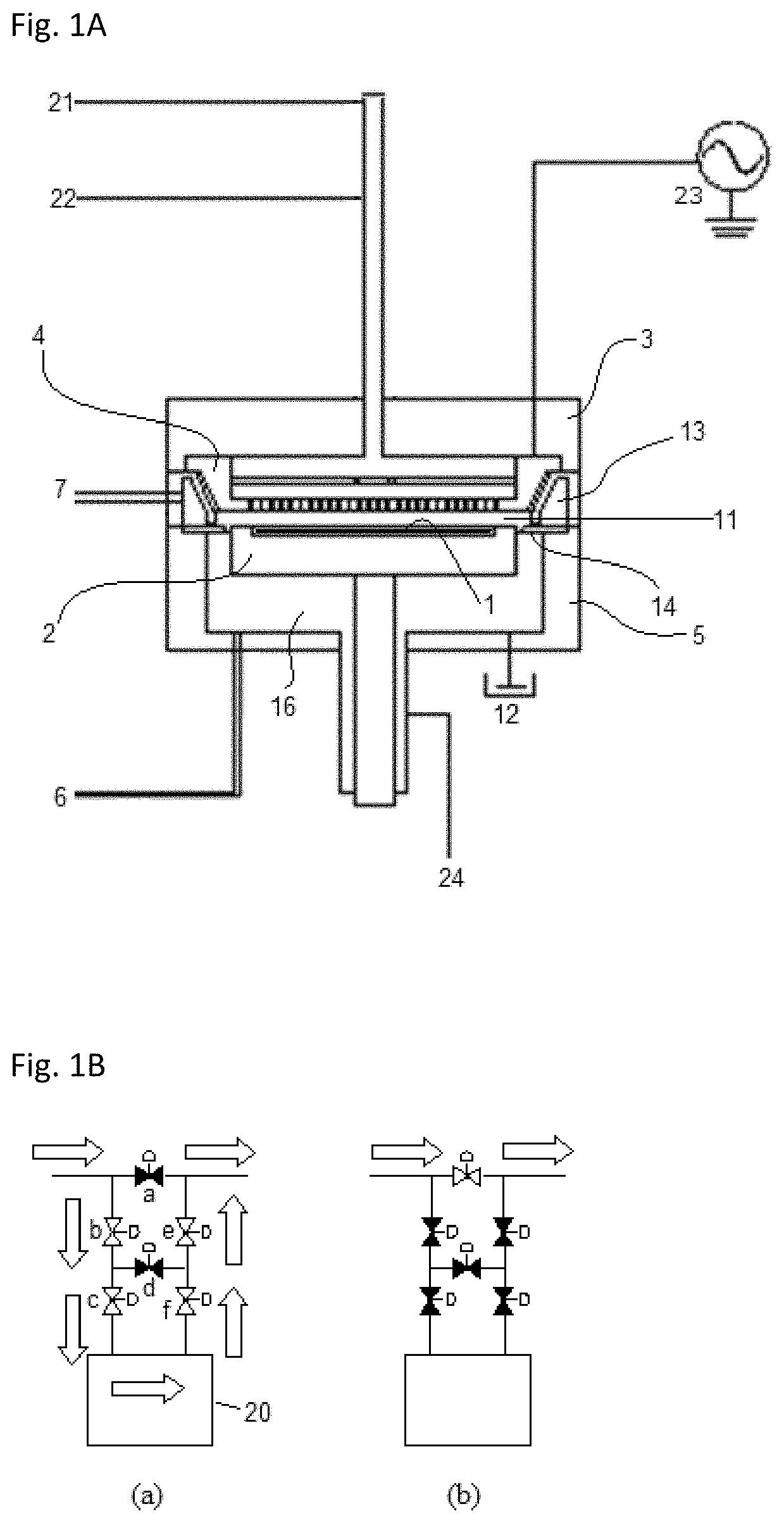
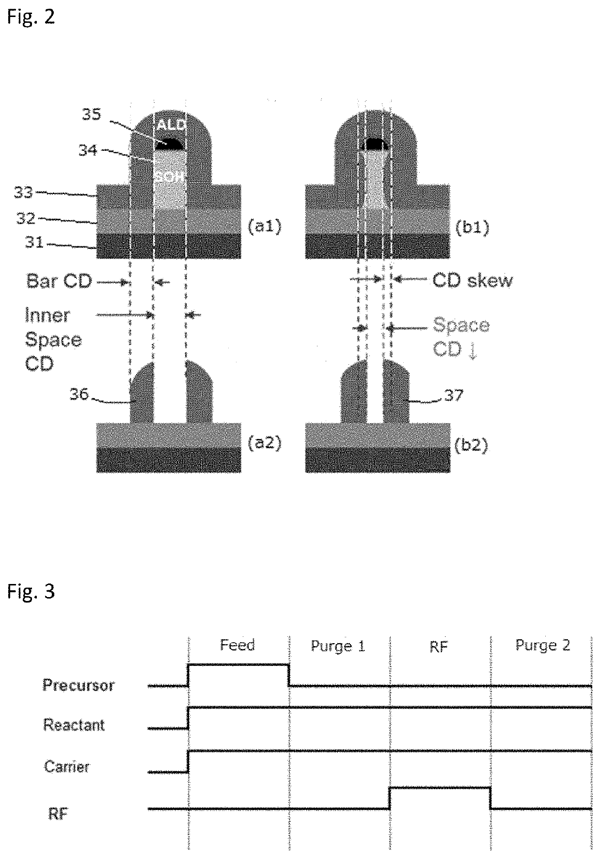
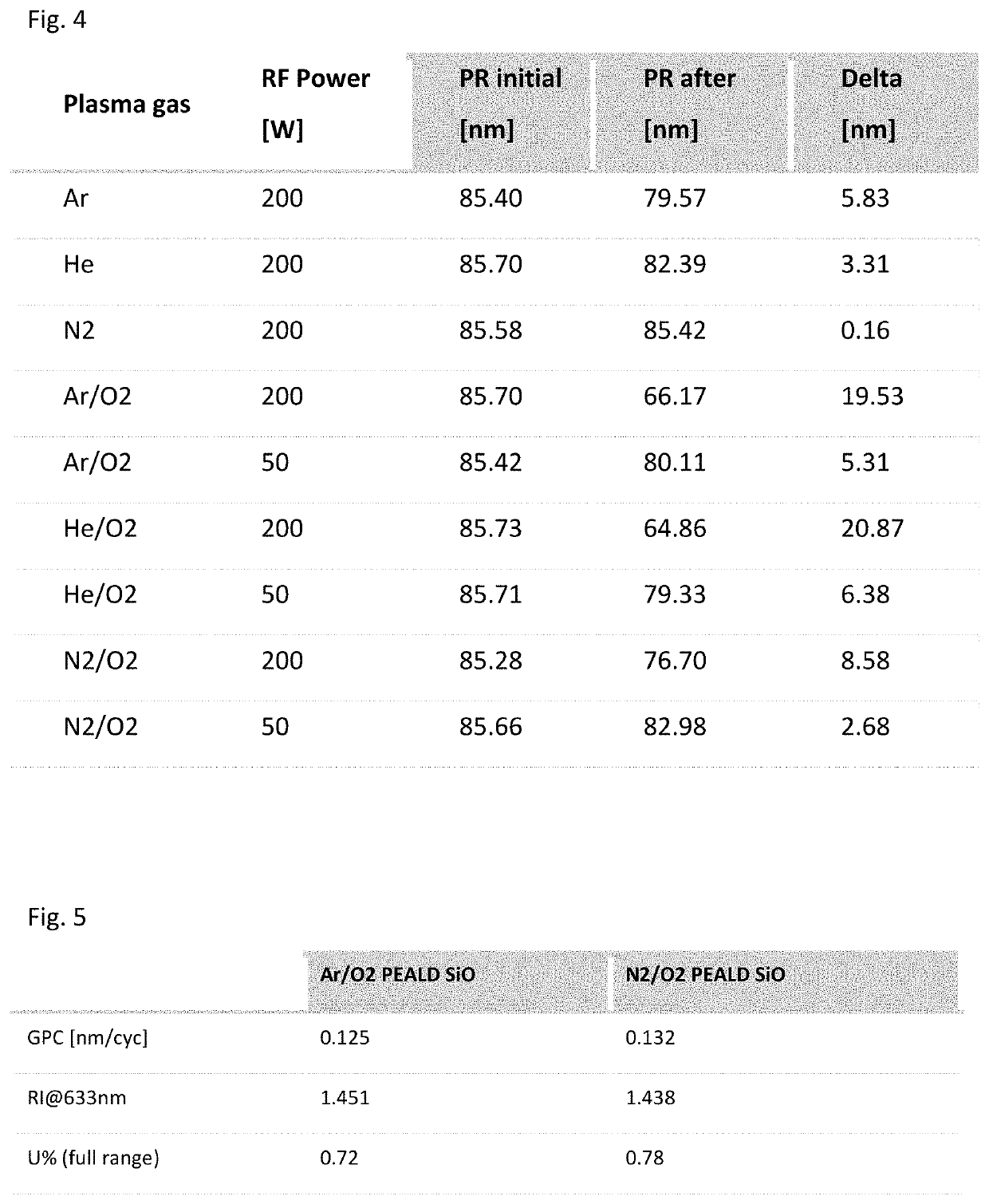
[0060]A photoresist layer (a blanket photoresist constituted by e.g., Novolacs designed for Argon Fluoride laser (ArF) lithography) was formed on a 300-mm substrate at a thickness which was considered to be an initial CD (“PR initial”) shown in FIG. 4, and then the substrate was loaded to an apparatus illustrated in FIG. 1A. The photoresist layer was exposed to a plasma using a gas shown in FIG. 4 (‘Plasma gas”) generated by applying RF power (13.56 MHz) shown in FIG. 4 (“RF Power”) under conditions shown in Table 2 below to evaluate plasma damage to the photoresist layer by measuring a reduction of the thickness of the layer after being exposed to the plasma. The results are shown in FIG. 4.

TABLE 2(numbers are approximate)Conditions for plasma exposureResist materialArF resistTemperature75° C.Pressure400 PaPlasma gasSee FIG. 4Plasma gas flowAr, He, N2 = 2 SLM;O2 = 0.5 SLMRF power for a 300-mm waferSee FIG. 4Duration10 secondsElectrode gap10 mm

[0061]As shown in FIG. 4, although all ...

reference example 2

[0062]A silicon oxide film (a blanket film) was deposited on a 300-mm substrate by PEALD in an apparatus illustrated in FIG. 1A with a flow-pass system (FPS) illustrated in FIG. 1B under conditions shown in Table 3 below to evaluate properties of a silicon oxide film deposited using an Ar / O2 plasma and those of a silicon oxide film deposited using a N2 / O2 plasma. The results are shown in FIG. 5.

TABLE 3(numbers are approximate)Conditions for PEALDTemperature of susceptor / 75° C. / 75° C. / 75° C.showerhead / wallElectrode gap10 mmPressure400 PaPrecursorBDEASReactantO2Carrier gas / Dilution gasEither Ar or N2Flow rate of reactant (continuous)500 sccmFlow rate of carrier gas (continuous)2 slmFlow rate of dilution gas (continuous)1 slmFlow rate of precursorCorresponding to the flow rate of carrier gasRF power (13.56 MHz) for a50 W300-mm waferDuration of “Feed”0.2 secDuration of “Purge 1”0.5 secDuration of “RF”0.4 secDuration of “Purge 2”0.1 secDuration of one cycle1.2 sec

[0063]As shown in FIG. 5...

reference example 3

[0065]Silicon oxide films were deposited on substrates, respectively, in a manner similar to that in Reference Example 2 under conditions shown in Table 4 blow. Thus-obtained silicon oxide films were subjected to composition analysis based on a Fourier Transform Infrared (FTIR) spectrum.

TABLE 4(numbers are approximate)Sample cSample aSample bO2(20%) / ArO2(20%) / N2O2(5%) / N2PrecursorBDEASSusceptor (° C.)75Wall (° C.)75Shower plate (° C.)75Feed / Purge / RF / Purge0.2 / 0.5 / 0.4 / 0.1 sPower (W)50Pressure (Pa)400 Gap (mm)10N2 (slm) Including033CarrierAr (slm) Including300CarrierO2 (slm)0.50.50.1Number of cycles100 (~12 nm)

[0066]FIG. 7 is a Fourier Transform Infrared (FTIR) spectrum of a SiO film formed in sample a, sample b, and sample c. As shown in FIG. 5, all the silicon oxide films show a SiO main peak, indicating that all the films were constituted by 5i0. Samples a and b had a weak peak at about 900 cm-1 which may be attributed to the presence of impurities such as NH2 and CH2, but is not bel...


PUM

PropertyMeasurementUnit
Timeaaaaaaaaaa
Flow rateaaaaaaaaaa
Flow rateaaaaaaaaaa

Abstract

A method of depositing an oxide film on a template for patterning in semiconductor fabrication, includes: (i) providing a template having patterned structures thereon in a reaction space; and (ii) depositing an oxide film on the template by plasma-enhanced atomic layer deposition (PEALD) using nitrogen gas as a carrier gas and also as a dilution gas, thereby entirely covering with the oxide film an exposed top surface of the template and the patterned structures.

Description

BACKGROUND OF THE INVENTIONField of the Invention[0001]The present invention generally relates to a method of depositing an oxide film on an underlying layer by plasma-enhanced atomic layer deposition (PEALD) without substantially damaging the underlying layer.Description of the Related Art[0002]Depositing a SiO2 film by PEALD is a method which can be conducted at a low temperature of e.g., 100° C. or lower and thus enables effective deposition of a conformal film on an organic film susceptible to heat by taking advantage of the low temperature deposition. This method is applied to patterning processes such as those by spacer-defined double patterning (SDDP) or spacer-defined quadruple patterning (SDQP) (more generally referred to as “SDxP”). However, conventional PEALD for depositing a SiO2 film uses a plasma of a mixed gas of Ar and O2, in which a photoresist is exposed to the plasma in the beginning of deposition until the photoresist is covered by a SiO2 film, thereby causing th...

Claims


Application Information

Patent Timeline
IPC IPC(8): H01L21/033C23C16/04C23C16/455C23C16/40H01L21/02H01L21/311
CPCH01L21/02274H01L21/31116H01L21/0332H01L21/0337H01L21/02183H01L21/0338C23C16/45553C23C16/401H01L21/0228H01L21/02164H01L21/02189H01L21/0335C23C16/042H01L21/02186C23C16/45536C23C16/40C23C16/405C23C16/45534C23C16/4554H01L21/02219C23C16/45525H01J37/32174H01L21/02554H01L21/306
Inventor ZAITSU, MASARUFUKAZAWA, ATSUKITRIGAGEMA, GAMA
Owner ASM IP HLDG BV
Why Eureka
Try Eureka