Switch device for switching an analog electrical input signal

a switch device and analog technology, applied in electronic switching, transistors, electrical apparatus, etc., can solve the problems of body-effect, non-linear input dependence of switch-resistance of the switch device during the on-state, and restrict the voltage swing on both the switched signals, so as to achieve simple and cost-effective implementation

Active Publication Date: 2020-04-23
FRAUNHOFER GESELLSCHAFT ZUR FOERDERUNG DER ANGEWANDTEN FORSCHUNG EV
View PDF0 Cites 0 Cited by
  • Summary
  • Abstract
  • Description
  • Claims
  • Application Information

AI Technical Summary

Benefits of technology

[0039]These features provide a simple and cost-effective implementation of the inventive switch device.

Problems solved by technology

However, the low break-down voltage of the thin gate-oxide and the low supply voltage due to the extensive scaling down in advanced CMOS processes, restrict the voltage swing on both the switched signal and the clock signal that drives the switch transistor.
This limits the performance of the MOSFET device as an analog switch device.
The design of reliable switch devices that can conduct as well as isolate while supporting sufficient signal swing has become a challenge.
This non-ideality manifests itself as non-linear settling error resulting in distortion.
Although known conventional bootstrap-ping techniques improve the analog switch performance to a large extent by making the gate-to-source-voltage of the switching transistor constant during conduction, the non-linear input dependence of the switch-resistance of the switch device during the on-state still prevails due to body-effect [4].
This leads to more parasitic components at the well-substrate junctions and also additional cost factor due to the requirement of an extra mask.
For a partially depleted silicon-on-insulator transistor the sandwiched film between the gate region and the insulator is large, so the depletion region can't cover the whole film.

Method used


Image

  • Switch device for switching an analog electrical input signal
  • Switch device for switching an analog electrical input signal
  • Switch device for switching an analog electrical input signal

Examples


Embodiment Construction

[0063]Equal or equivalent elements or elements with equal or equivalent functionality are denoted in the following description by equal or equivalent reference numerals.

[0064]In the following description, a plurality of details is set forth to provide a more thorough explanation of embodiments of the present disclosure. However, it will be apparent to those skilled in the art that embodiments of the present disclosure may be practiced without these specific details. In other instances, well-known structures and devices are shown in block diagram form rather than in detail in order to avoid obscuring embodiments of the present disclosure. In addition, features of the different embodiments described hereinafter may be combined with each other, unless specifically noted otherwise.

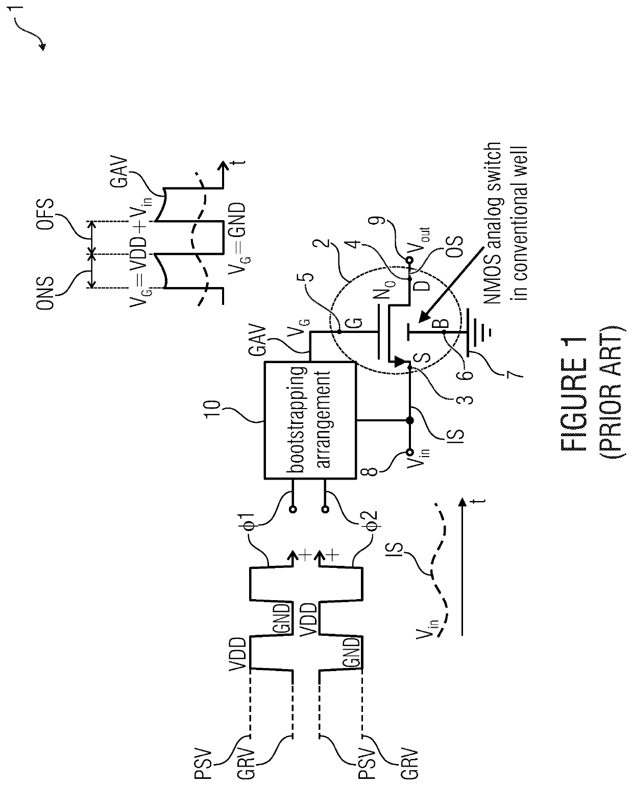
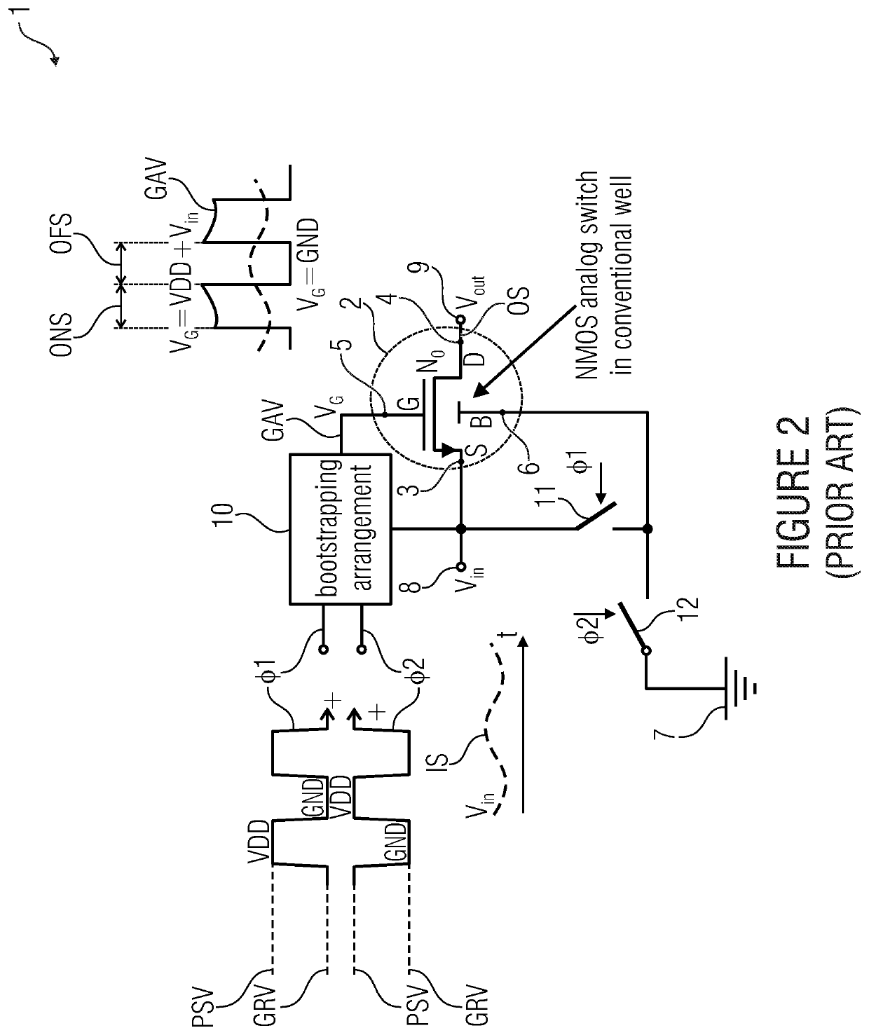
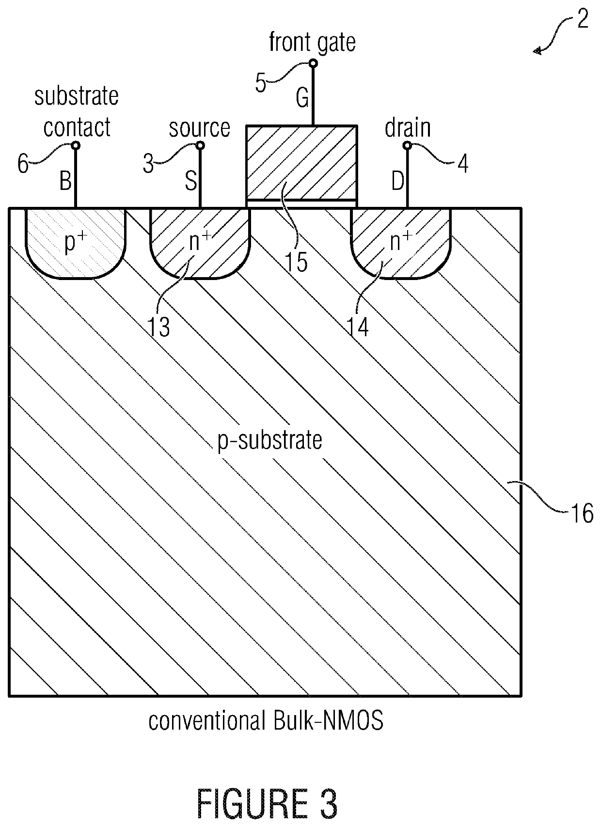
[0065]FIG. 1 illustrates a first embodiment of a switch device 1 for switching an analog electrical input signal IS according to conventional technology in a schematic view. The switch device 1 comprises a swi...


PUM

PropertyMeasurementUnit
voltageaaaaaaaaaa
aspect ratioaaaaaaaaaa
voltageaaaaaaaaaa

Abstract

A switch device for switching an analog electrical input signal includes: a switching transistor being a flipped-well-silicon-on-insulator-NMOS transistor; and a bootstrapping arrangement including a voltage providing arrangement for providing a floating voltage during the on-state, wherein the floating voltage is provided at a positive terminal and at a negative terminal of the voltage providing arrangement; wherein the bootstrapping arrangement is configured in such way that during the on-state the positive terminal is electrically connected to the front gate contact of the switching transistor and to the back gate contact of the switching transistor, and the negative terminal is electrically connected to the source contact of the switching transistor; wherein the bootstrapping arrangement is configured in such way that during the off-state the positive terminal and the negative terminal are not electrically connected to the switching transistor.

Description

CROSS-REFERENCES TO RELATED APPLICATIONS[0001]This application is a continuation of copending International Application No. PCT / EP2018 / 069156, filed Jul. 13, 2018, which is incorporated herein by reference in its entirety, and additionally claims priority from European Application No. EP 17181434.6, filed Jul. 14, 2017, which is incorporated herein by reference in its entirety.BACKGROUND OF THE INVENTION[0002]The performance of many types of time-discrete circuits, such as switched-capacitor circuits, depends on the linearity of their analog switch transistor. A simple MOSFET device offers the functionality of such an analog switch transistor that can be controlled by a clock signal to either conduct or block signal-transfer between its source and drain terminals. However, the low break-down voltage of the thin gate-oxide and the low supply voltage due to the extensive scaling down in advanced CMOS processes, restrict the voltage swing on both the switched signal and the clock signa...

Claims


Application Information

Patent Timeline
Patent Type & Authority Applications(United States)
IPC IPC(8): H03K17/16H03K17/10H03K17/284H03K17/687
CPCH03K17/102H03K17/08H03K17/284H03K17/687H03K17/161H03K17/063H03K2217/0018H03K2217/0054
Inventor BORA, PRAGOTI PRANBORGGREVE, DAVIDVANSELOW, FRANK
Owner FRAUNHOFER GESELLSCHAFT ZUR FOERDERUNG DER ANGEWANDTEN FORSCHUNG EV
Why Eureka
Try Eureka