Thermal processing method for silicon wafer

Active Publication Date: 2020-06-11
GLOBALWAFERS JAPAN
0 Cites 0 Cited by

AI-Extracted Technical Summary

Problems solved by technology

However, an infrared scattering tomography apparatus can detect only oxygen precipitates having sizes of about 25 nm or more, and it is difficult to detect any smaller oxygen precipitates.
For example, it has been found that, in an image sensor device, oxygen precipitates equal to or smaller in size than the lower detection limit of an infrared scattering tomography apparatus may cause pixel defects of the image sensor called “white spot defects”, and suppression of minute oxygen precipitates undetectable by an infrared scattering tomography apparatus is becoming more important.
However, the VOx density is difficult to measure unless a special method requiring a high cost such as DLTS measurement after platinum diffusio...

Method used

[0074]Next, handling of oxygen atoms and nitrogen atoms in a silicon single crystal will be described. In a silicon single crystal manufactured by the CZ method, a quartz crucible holding a silicon melt at the time of pulling melts into a silicon melt, and oxygen atoms are taken in. Such oxygen atoms are transported to just below the growth interface of the silicon single crystal due to convection of the melt and diffusion in the melt and is mixed into the silicon single crystal from the growth interface. Nitrogen atoms are intentionally added to the silicon melt as a silicon nitride film or the like in order to suppress the size of void defects generated in the silicon single crystal. Normally, these atoms diffuse in the silicon single crystal based on the following Formulae (14) and (15).
[0094]After the RTP was actually performed under the thermal processing conditions described above, thermal processing was performed for revealing oxygen precipitates at 780° C. for three hours followed by 1000° C. for 16 hours. FIGS. 5A to 7C show measurement results of the wafer depth direction distribution of oxygen precipitates using an infrared scattering tomography apparatus (MO441; manufactured by Raytex Corporation). FIGS. 5A to 5C correspond to the simulation result marked with V in FIG. 4, FIGS. 6A to 6C correspond to the simulation result marked with VI in FIG. 4, and FIGS. 7A to 7C correspond to the simulation results marked with VII in FIG. 4. From the comparison of these simulation results and actual measurement results of the wafer depth direction distribution of oxygen precipitates, it was confirmed that the wafer depth direction distribution of oxygen precipitates can be accurately controlled by adjusting the depth direction distribution of the VOx density according to the RTP conditions.
[0101]As described above, by performing simulation using the RTP conditions (processing temperature, cooling rate, oxygen partial pressure) as parameters, it is possible to conveniently derive the wafer depth direction distribution of the VOx density which is very difficult to directly evaluate, and it is possible to conveniently determine pr...

Benefits of technology

[0022]In the present invention, a thermal processing method for a silicon wafer, wherein a processing temperature TS by a rapid thermal processing device is 1250° C. or more and 1350° C. or less, and a cooling rate Rd from the processing temperature TS is in a range of 20° C./s or more and 150° C./s or less, an upper limit and a lower limit of an oxygen partial pressure P in a thermal processing atmosphere gas are represented by predetermined formulae, and thermal processing is performed within a range between the upper limit...

Abstract

A processing temperature TS by a rapid thermal processing furnace is 1250° C. or more and 1350° C. or less, and a cooling rate Rd from the processing temperature is in a range of 20° C./s or more and 150° C./s or less, and thermal processing is performed by adjusting the processing temperature TS and the cooling rate Rd within a range between the upper limit P=0.00207TS·Rd−2.52Rd+13.3 (Formula (A)) and the lower limit P=0.000548TS·Rd−0.605Rd−0.511 (Formula (B)) of an oxygen partial pressure P in a thermal processing atmosphere.

Application Domain

Polycrystalline material growthAfter-treatment details +2

Technology Topic

PhysicsSilicon chip +6

Image

  • Thermal processing method for silicon wafer
  • Thermal processing method for silicon wafer
  • Thermal processing method for silicon wafer

Examples

  • Experimental program(1)

Example

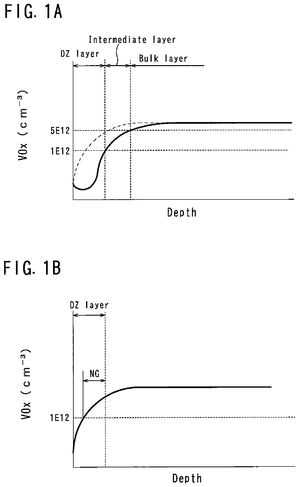
[0054]A thermal processing method for a silicon wafer (wafer) according to the present invention is a method for performing rapid thermal processing (RTP) by using a ramp annealing furnace capable of rapidly increasing and decreasing temperature in an oxygen atmosphere (oxygen partial pressure is in the range of 1% or more and 100% or less) and for introducing vacancy oxygen complexes (VOx), which are complexes of vacancies and oxygen, into the wafer. As the wafer for thermal processing, a wafer sliced from an ingot grown by the Czochralski method (hereinafter referred to as CZ method) and mirror polished on both sides thereof is used.
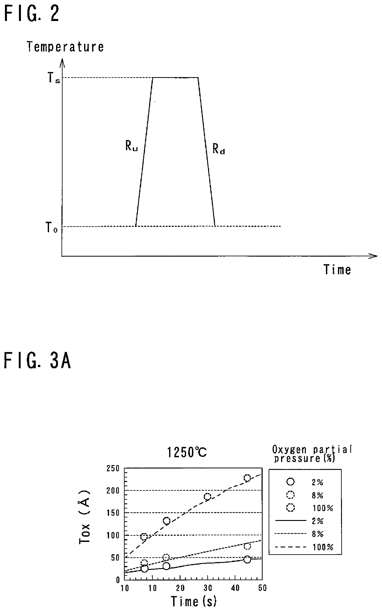
[0055]As the RTP thermal processing, for example, a sequence shown in FIG. 2 is employed. In this sequence, the temperature is raised at a predetermined ramp up rate Ru from a predetermined temperature T0 (for example, 700° C.) to a processing temperature TS, and is held for a predetermined time (for example, 15 seconds) at the processing temperature TS. Then, the temperature is decreased from the processing temperature TS to the predetermined temperature T0 at a predetermined cooling rate Rd.
[0056]The VOx density distribution in the wafer depth direction was calculated using a point defect simulation. The point defect simulation is a model of a series of physical phenomena comprising formation of an oxide film on the surface of the wafer by thermal processing in an oxygen atmosphere, generation of interstitial silicon atoms at the interface between the oxide film and the silicon crystal, diffusion of the interstitial silicon atoms into the wafer, and pair annihilation of the interstitial silicon atoms and vacancies. In the following, the point defect simulation will be described in detail, and a method of determining the upper and lower limits of the oxygen partial pressure or predicting the widths of the DZ layer and the intermediate layer by regression analysis from the results of this simulation will be described.
[0057](1) Regarding Point Defect Simulation
(a) Formation of Oxide Film
[0058]When RTP is performed in an oxygen atmosphere, an oxide film is formed as described above, and interstitial silicon atoms are injected into the wafer from the interface between the oxide film and the silicon crystal. It is known that the ratio of the concentration of interstitial silicon atoms generated at the interface between the oxide film and the silicon crystal to the thermal equilibrium concentration thereof in the silicon crystal, that is, the degree of supersaturation of interstitial silicon atoms, is a factor which greatly influences the accuracy of point defect simulation, and is known to be determined by the growth rate of the oxide film. Therefore, the growth rate of the oxide film during RTP in an oxygen atmosphere will be examined in detail.
[0059]Growth of the oxide film is represented by the Deal-Grove equation (B. Deal, J. Electrochem. Soc. 125 (1978) 576) shown in Formula (1).
[Math. 5]
X02+AX0=B(t−t0)  (1)
[0060]Here, X0 is the thickness of the oxide film, t is the time, and to is the time expressing the initial value of the thickness of the oxide film. When the oxide film is sufficiently thick, Formula (1) is approximated as the following Formula (1′), and the thickness X0 of the oxide film becomes a parabolic function proportional to the root of time.
[Math. 6]
X20=Bt (1′)
[0061]Here, the following Formula (2) is obtained by differentiating Formula (1).
[ Math . 7 ] ( d X 0 d t ) - 1 = 1 B / A + 2 X 0 B = 1 K L + 2 X 0 K P ( 2 )
[0062]Here, B/A is called Linear rate constant (KL), and B is called Parabolic rate constant (KP). B/A corresponds to a reaction rate at the oxide film-wafer interface, and B relates to the thickness of the oxide film, and is a term corresponding to a diffusion effect in the oxide film. Although, inherently, Formula (2) is an equation to be applied to the entire oxidation process including the process of increasing the oxide film thickness, Kotani et al. showed that Formula (2) itself is usable also for the initial process of oxidation in which only a thin oxide film is formed such as during RTP by replacing the values of KL and KP with values for RTP (Y. Kotani and Y. Omura, Jpn. J. Appl. Phys. 39 (2000) 4549).
[0063]Since data during RTP in an oxygen atmosphere obtained by Kotani et al. is up to 1100° C., for the temperature region higher than 1100° C., thickness data of the oxide film when changing the processing temperature, the processing time, and the oxygen partial pressure of RTP was obtained by an experiment. Plots shown in FIGS. 3A to 3D are data obtained by such an experiment. The oxidation rate was calculated from these data and KL and KP were determined as a function of temperature and oxygen partial pressure as shown in the following Formulae (3) and (4).
[Math. 8]
KL=629P0.6 exp(−0.5437 eV/kT)(A/s)  (3)
[Math. 9]
KP=1.01×10¹¹P0.6 exp(−2.347 eV/kT)(A2/s)  (4)
[0064]Here, P represents the oxygen partial pressure during RTP in an oxygen atmosphere, and T represents the absolute temperature. Calculated values of the thickness of the oxide film obtained from Formulae (2), (3), and (4) are indicated by lines in FIGS. 3A to 3D. These calculated values and experimental data are in good agreement with each other, indicating that the oxidation rate at any processing temperature and oxygen partial pressure can be accurately estimated from the values of KL and KP determined by the processing temperature and oxygen partial pressure.
[0065](b) Calculation of VOx Density
[0066]The density distribution of VOx formed in the wafer was calculated by the following procedure.
[0067]The growth rate of the oxide film formed on the wafer surface can be expressed by the following Formula (2′) from Formula (2).
[ Math . 10 ] d X 0 d t = 1 1 / K L + 2 X 0 / K P ( 2 ′ )
[0068]The thickness of the oxide film at any time during the RTP process was determined by integrating Formula (2′) over the entire process of RTP while increasing the temperature, while holding the processing temperature, and while decreasing the temperature. In this integration, the film thickness of a natural oxide film was defined as the initial thickness of the oxide film. The values of Formulae (3) and (4) were employed as values of KL and KP in Formula (2′). From these, the growth rate of the oxide film at an arbitrary time was obtained using Formula (2′). Using the obtained growth rate of the oxide film, the supersaturation degree of interstitial silicon atoms at the interface between the oxide film and the wafer was obtained by the following Formula (5) proposed by Taniguchi et al. (K. Taniguchi et al., J. Appl. Phys. 65 (1989) 2723).
[ Math . 11 ] C I C I eq = A 1 ( d X 0 / d t ) + A 2 ( d X 0 / d t ) 0.5 + A 2 ( 5 )
[0069]Here, CI is the concentration of the interstitial silicon atoms, CIeq is the thermal equilibrium concentration of the interstitial silicon atoms, and A1 and A2 are parameters related to the oxidation phenomenon. A1 and A2 in a dry oxygen atmosphere were determined to fit to the relationship between the supersaturation degree of interstitial silicon atoms and the growth rate of the oxide film determined experimentally by Dunhum (S. T. Dunhum, J. Appl. Phys. 71 (1992) 685). The density of interstitial silicon atoms generated at the oxidation interface is obtained by multiplying the degree of supersaturation of interstitial silicon atoms obtained from Formula (5) by the thermal equilibrium concentration of interstitial silicon atoms described below.
[0070]The vacancy concentration CV at the interface between the oxide film and the silicon crystal was determined from the following Formula (6) representing a local equilibrium relationship assuming that the relationship of generation/pair annihilation of vacancies V and interstitial silicon atoms I is in a steady state balance.
[Math. 12]
CVCI=CVeqCIeq (6)
[0071]Here, CV is the concentration of vacancies, and CVeq is the thermal equilibrium concentration of vacancies. As can be seen from Formula (6), the CV at the oxide film-Si crystal interface is determined by the CI at this interface. The point defect concentration in the wafer is determined by solving the following Formulae (7) and (8) with the CV and the CI at the interface as boundary conditions.
[ Math . 13 ] ∂ C V ∂ t = D V ∂ 2 C V ∂ Z 2 - K IV ( C V C I - C V eq C I eq ) ( 7 ) [ Math . 14 ] ∂ C I ∂ t = D I ∂ 2 C I ∂ Z 2 - K IV ( C V C I - C V eq C I eq ) ( 8 )
[0072]Here, DV is the diffusion coefficient of vacancies, DI is the diffusion coefficient of the interstitial silicon atoms, and KIV is the reaction constant of the pair annihilation reaction of vacancies and interstitial silicon atoms. This reaction constant K can be represented by the following Formula (9).
[Math. 15]
KIV=4πac(DV+DI)exp(−ΔGIV/kT)  (9)
[0073]Here, ac is the critical distance at which the vacancies V and the interstitial silicon atoms I cause pair annihilation, and ΔGIV is the barrier energy of annihilation. In this calculation, the same numerical values as used by Kissinger et al., or ac=0.543 nm and ΔGIV=0 were employed (G. Kissinger et al., J. Electrochem. Soc. 154 (2007) H4547). For the diffusion coefficient and thermal equilibrium concentrations of vacancies and interstitial silicon atoms, the values used by Nakamura et al. shown in Formulae (10)-(13) were employed (K. Nakamura et al., in Semiconductor Silicon, PV2002-2, p. 554, The Electrochemical Society Proceedings Series, Pennington, N.J. (2002)).
[Math. 16]
DV=3.5×10⁻⁴ exp(−0.3 eV/kT)(cm2/s)  (10)
[Math. 17]
DI=2.45×10⁻¹ exp(−0.9 eV/kT)(cm2/s)  (11)
[Math. 18]
CVeq=3.85×1026 exp(−3.94 eV/kT)(cm−3)  (12)
[Math. 19]
CIeq=6.12×1026 exp(−4.05 eV/kT)(cm−3)  (13)
[0074]Next, handling of oxygen atoms and nitrogen atoms in a silicon single crystal will be described. In a silicon single crystal manufactured by the CZ method, a quartz crucible holding a silicon melt at the time of pulling melts into a silicon melt, and oxygen atoms are taken in. Such oxygen atoms are transported to just below the growth interface of the silicon single crystal due to convection of the melt and diffusion in the melt and is mixed into the silicon single crystal from the growth interface. Nitrogen atoms are intentionally added to the silicon melt as a silicon nitride film or the like in order to suppress the size of void defects generated in the silicon single crystal. Normally, these atoms diffuse in the silicon single crystal based on the following Formulae (14) and (15).
[ Math . 20 ] ∂ C O ∂ t = D O ∂ 2 C O ∂ Z 2 ( 14 ) [ Math . 21 ] ∂ C N ∂ t = D N ∂ 2 C N ∂ Z 2 ( 15 )
[0075]Here, CO is the concentration of oxygen atoms and CN is the concentration of nitrogen atoms. DO is the diffusion coefficient of oxygen, and DN is the diffusion coefficient of nitrogen, which are given by the following Formulae (16) and (17), respectively, by Mikkelesen et al. (J. C. Mikkelsen, Jr., in Oxygen, Carbon, Hydrogen and Nitrogen in Crystalline Silicon, ed. J. C. Mikkelsen, Jr. et al. (MRS, Princeton, N. J., 1986) 19), and Y. Itoh et al. (Y. Itoh, T Abe, Appl Phys. Lett.) vol53 (1988) 39).
[Math. 22]
DO=0.13 exp(−2.53 eV/kT)(cm2/s)  (16)
[Math. 23]
DN=2.7×10³ exp(−2.8 eV/kT)(cm2/s)  (17)
[0076]It is assumed that the concentrations of oxygen and nitrogen atoms at the interface between the oxide film and silicon crystal have thermal equilibrium concentrations represented by the following Formulae (18) and (19), respectively.
[ Math . 24 ] C O eq = 2.0 × 10 21 exp ( - 1.03 e V / k T ) ( cm - 3 ) ( 18 ) [ Math . 25 ] C N eq = 4.5 × 10 15 exp ( - 2.15 e V / k ( 1 T - 1 1685 ) ) ( cm - 3 ) ( 19 )
[0077]Here, COeq is the thermal equilibrium concentration of oxygen and CNeq is the thermal equilibrium concentration of nitrogen. As the thermal equilibrium concentration of nitrogen atoms, an energy value of 2.15 eV employed by Voronkov et al. was used (V. V. Voronkov and R. Falster, J. Electrochem. Soc. 149 (2002) G167).
[0078]Nitrogen atoms and vacancies in the silicon single crystal easily form complexes (hereinafter referred to as NV complexes) during the cooling process. This density is given by the following Formula (20) according to Voronkov et al.
[Math. 26]
[NV]=CV/CVeq[N2]1/2 exp(−EneV/kT)(cm−3)  (20)
[0079]Here, the value in [ ] in Formula (20) represents the atomic fraction, and [NV]=CNV/ρ, and [N2]=CN2/ρ. ρ represents the atomic density of the silicon single crystal, and ρ=5×10²²/Cm3. In this calculation, it is assumed that the NV complexes do not diffuse.
[0080]A steady state balance is always established between the concentrations of vacancies V, nitrogen N2, and NV complexes in the silicon single crystal. In other words, assuming that the total vacancy concentration is CVT and its thermal equilibrium concentration is CVT·eq, relationships of the following Formulae (21) and (22) are established.
[Math. 27]
CVT=CV+CNV (21)
[Math. 28]
CVT·eq=CVeq+CNVeq (22)
[0081]Here, the vacancy concentration CV and the NV complex concentration CNV are determined from the total vacancy concentration CVT in each element space by using the following Formulae (23) and (24).
[Math. 29]
CV=(CVeq/CVT·eq)CVT (23)
[Math. 30]
CNV=(CVeq/CVT·eq)CVT (24)
[0082]Here, when Formula (23) is modified, the following Formula (25) is obtained.
[Math. 31]
CV/CVeq=CVT/CVT·eq (25)
[0083]By substituting Formula (25) into Formula (24), the following Formula (26) is obtained.
[Math. 32]
CNV=CNVeq(CV/CVeq)  (26)
[0084]Since CNVeq is represented by the following Formula (27), Formulae (20) and (26) coincide.
[Math. 33]
CNVeq=ρ(CN2/ρ)1/2 exp(−En/kT)  (27)
[0085]The Formula (27) represents the thermal equilibrium concentration of the NV complexes when the vacancy concentration is the thermal equilibrium concentration.
[0086]In a point defect simulation after RTP in an oxygen atmosphere, first, as the initial state, thermal equilibrium concentrations of vacancies and interstitial silicon atoms corresponding to the initial temperature of RTP are given over the entire depth direction of the wafer. Then, the thermal equilibrium concentrations given by Formulae (5) and (6) are changed as boundary conditions between the oxide film and the silicon crystal, corresponding to each temperature change while the ramp up, while the duration at maximum temperature, and while the cooling in RTP. Along with this, the wafer depth direction distribution of vacancies and interstitial silicon atoms is derived by numerical calculation by using Formulae (7)-(9).
[0087]As in the calculation of vacancies and interstitial silicon atoms, firstly, as an initial state, the concentration of oxygen atoms and the concentration of nitrogen atoms corresponding to the initial temperature of RTP are given over the entire depth direction of the wafer. Then, the thermal equilibrium concentrations given in Formulae (18) and (19) are changed as boundary conditions of the concentrations of oxygen atoms and nitrogen atoms between the oxide film and the silicon crystal corresponding to each temperature change while the ramp up, while the duration at maximum temperature, and while the cooling in RTP. Along with this, the wafer depth direction distribution of oxygen and nitrogen is derived by numerical calculation using Formulae (14)-(17).
[0088]Regarding the interaction between nitrogen atoms and vacancies, the concentration ([NV]) of the complexes of nitrogen and vacancies is calculated using Formulae (20)-(27). In calculating the vacancy concentration, considering that the nitrogen-vacancy complexes (NV) rapidly diverge (NV→N+V) due to the decrease of independently present single vacancies (V), and becomes a source of single vacancies, the total vacancy concentration was calculated as the sum ([V]+[NV]) of the single vacancy concentration ([V]) and the nitrogen-vacancy complex concentration ([NV]).
[0089]During the cooling step of RTP, more specifically at 1000° C. or lower, it was assumed that the total vacancies rapidly react with oxygen atoms present in the wafer at a concentration several orders of magnitude higher than the vacancies, and change to VOx's which are most stable at a low temperature. In other words, in this point defect simulation, it was assumed that the total vacancy concentration and the VOx density correspond one-to-one.
[0090]FIG. 4 shows an example of the simulation result of the wafer depth direction distribution of VOx's when the processing temperature, the cooling rate, and the oxygen partial pressure during RTP were varied. The region where the VOx density is less than 1.0×10¹²/cm3 corresponds to the DZ layer, the region where the VOx density is 5.0×10¹²/cm3 or more corresponds to the bulk layer, and the region where the VOx density is 1.0×10¹²/cm3 or more and less than 5.0×10¹²/cm3 corresponds to the intermediate layer.
[0091]From the simulation results marked with V in FIG. 4, it is apparent that the higher the cooling rate, the shallower the width of the DZ layer, and the more steeply the VOx density rises. This is because as the cooling rate increases, a sufficient time is not given for vacancies to outwardly diffuse to the front side of the wafer during RTP, and the region having a high VOx density remains near the surface of the wafer.
[0092]From the simulation results marked with VI and VII in FIG. 4, it was found that the higher the processing temperature, the higher the VOx density. This is because the higher the temperature, the higher the thermal equilibrium density of vacancies and more VOx's are frozen in the wafer by RTP.
[0093]Furthermore, from the comparison of the simulation results marked with V and the simulation results marked with VI and VII in FIG. 4, it was found that the width of the DZ layer was wider when the oxygen atmosphere (here, the oxygen partial pressure is 100%) was used than when the atmosphere containing no oxygen (0% oxygen partial pressure) was used. This is because in the oxygen atmosphere, as described above, interstitial silicon atoms are injected into the wafer surface layer from the interface between the oxide film and the silicon crystal, and pair annihilation of the vacancies and the interstitial silicon atoms decreases the VOx density.
[0094]After the RTP was actually performed under the thermal processing conditions described above, thermal processing was performed for revealing oxygen precipitates at 780° C. for three hours followed by 1000° C. for 16 hours. FIGS. 5A to 7C show measurement results of the wafer depth direction distribution of oxygen precipitates using an infrared scattering tomography apparatus (MO441; manufactured by Raytex Corporation). FIGS. 5A to 5C correspond to the simulation result marked with V in FIG. 4, FIGS. 6A to 6C correspond to the simulation result marked with VI in FIG. 4, and FIGS. 7A to 7C correspond to the simulation results marked with VII in FIG. 4. From the comparison of these simulation results and actual measurement results of the wafer depth direction distribution of oxygen precipitates, it was confirmed that the wafer depth direction distribution of oxygen precipitates can be accurately controlled by adjusting the depth direction distribution of the VOx density according to the RTP conditions.
[0095]A semiconductor device was formed on each of wafers shown in FIGS. 5A to 5C subjected to RTP under conditions of the cooling rates of 120° C./s (see FIG. 5A), 50° C./s (see FIG. 5B), and 25° C./s (see FIG. 5C), and the electrical characteristics of each semiconductor device were evaluated. As a result, the electrical characteristics of a semiconductor device formed in a region close to the surface (region shallower than about 60 μm) of any of the wafers were considerably favorable. In contrast, when a semiconductor device was formed in a region deeper than about 60 μm of a wafer subjected to RTP at a cooling rate of 120° C./s, when a semiconductor device was formed in a region deeper than about 90 μm of a wafer subjected to RTP at a cooling rate of 50° C./s, and when a semiconductor device was formed in a region (region having a VOx density of 1.0×10′2/cm3 or more and denoted as “NG” in FIG. 4) deeper than about 130 μm of a wafer subjected to RTP at a cooling rate of 25° C./s, it was confirmed that the electrical characteristics of the semiconductor device tended to be inferior.
[0096]Further, FIG. 8 is a diagram showing simulation results of the wafer depth direction distribution of the VOx density when the processing temperature was changed under five conditions ranging from 1350 to 1150° C. (at 50° C. pitch), the ramp up rate was set to 75° C./s, the cooling rate was changed under four conditions of 120, 50, 25, and 5° C./s, and the oxygen partial pressure was changed under 10 conditions of 100, 50, 30, 10, 8, 6, 4, 2, 1, and 0% (under total of 200 conditions combining all conditions), and FIG. 9 is a diagram showing simulation results of the wafer depth direction distribution of the VOx density variation amount in the wafer depth direction (depth differentiation of the VOx's) in the simulation of FIG. 8.
[0097]According to the simulation result of FIG. 8, as described in FIG. 4, under conditions which the cooling rate and the oxygen partial pressure were fixed, although there were some exceptions, the higher the processing temperature, the higher the VOx density. Under conditions which the processing temperature and oxygen partial pressure were fixed, the higher the cooling rate, the higher the VOx density. Further, under conditions which the processing temperature and cooling rate were fixed, the higher the oxygen partial pressure, the lower the VOx density.
[0098]As described above, when the region having a VOx density of less than 1.0×10′2/cm3 is defined as the DZ layer, the region having a VOx density of 1.0×10¹²/cm3 or more and less than 5.0×10¹²/cm3 is defined as the intermediate layer, and the region having a VOx density of 5.0×10¹²/cm3 or more is defined as the bulk layer, whether or not each of these layers is formed by RTP and the thickness of each layer formed by RTP largely change depending on the processing conditions of RTP.
[0099]As shown in FIG. 8, for example, when RTP is performed under the conditions of a processing temperature of 1350° C., a ramp up rate of 75° C./s, a cooling rate of 120° C./s, and an oxygen partial pressure of 30%, a DZ layer with a thickness of about 15 μm is formed on the wafer, and an intermediate layer with a thickness of about 50 μm is formed on the wafer. When RTP is performed under conditions of a processing temperature of 1350° C., a ramp up rate of 75° C./s, a cooling rate of 50° C./s, and an oxygen partial pressure of 10%, a DZ layer of about 4 μm is formed on the wafer and an intermediate layer having a thickness of about 59 μm is formed on the wafer.
[0100]In contrast, for example, when RTP is performed on a wafer under conditions of a processing temperature of 1350° C., a ramp up rate of 75° C./s, a cooling rate of 120° C./s, and an oxygen partial pressure of 10%, no DZ layer is formed, and when RTP is performed on a wafer under conditions of a processing temperature of 1350° C., a ramp up rate of 75° C./s, a cooling rate of 5° C./s, and an oxygen partial pressure of 30%, no intermediate layer and no bulk layer are formed, in any of the above cases, the wafer is unusable as a substrate for semiconductor devices.
[0101]As described above, by performing simulation using the RTP conditions (processing temperature, cooling rate, oxygen partial pressure) as parameters, it is possible to conveniently derive the wafer depth direction distribution of the VOx density which is very difficult to directly evaluate, and it is possible to conveniently determine processing conditions of a wafer having a DZ layer and an intermediate layer having desired thicknesses.
[0102]According to the simulation result of FIG. 9, under conditions which the cooling rate and oxygen partial pressure were fixed, although there are some exceptions, the higher the processing temperature, the higher the maximum value of the amount of change (differential value) of the VOx density in the wafer depth direction, and the position of the maximum value moved to the vicinity of the surface of the wafer. Under conditions which the processing temperature and oxygen partial pressure were fixed, the higher the cooling rate, the higher the maximum value of the differential value, and the maximum value moved to the vicinity of the surface of the wafer. Further, under conditions which the processing temperature and the cooling rate were fixed, when the oxygen partial pressure was around 10%, the maximum value of the differential value was the largest, and when the oxygen partial pressure was lower or higher than about 10%, the maximum value was lower. As the oxygen partial pressure increased, the maximum value moved toward the center of the thickness of the wafer.
[0103]The rise of the VOx density in the intermediate layer becomes steeper as the maximum value of the differential value becomes larger, so that the DZ layer and the bulk layer can be brought closer to each other via the intermediate layer. In this way, by bringing these layers close to each other, the diffusion length of heavy metals can be shortened, and gettering can be performed efficiently. By setting the position of the maximum value near the surface of the wafer, it is possible to efficiently getter in the same manner as described above even for heavy metals such as molybdenum, tungsten, and cobalt which have a small diffusion coefficient and are difficult to getter.
[0104](2) Regarding Regression Analysis (a) Determination of Upper Limit and Lower Limit of Oxygen Partial Pressure
[0105]From the simulation results shown in FIG. 8, data of a wafer including both a DZ layer with high integrity and a bulk layer with high gettering ability or data of a wafer thermally processed at RTP conditions (processing temperature, cooling rate, and oxygen partial pressure) in which the VOx density of the DZ layer is less than 1.0×10¹²/cm3 and the VOx density of the bulk layer is 5.0×10¹²/cm3 or more was picked up and plotted in FIGS. 10A to 10C. FIG. 10A shows the results when the processing temperature was 1250° C., FIG. 10B shows the results when the processing temperature was 1300° C., and FIG. 10C shows the results when the processing temperature was 1350° C.
[0106]Next, a regression equation composed of three parameters of processing temperature TS, cooling rate Rd, and oxygen partial pressure P was derived in such a manner that the picked-up RTP conditions were included. This regression equation is composed of the equation (A) representing the upper limit of the oxygen partial pressure P and the equation (B) showing the lower limit of the oxygen partial pressure P.
[Math. 34]
P=0.00207TS·Rd−2.52Rd+13.3  (A)
[Math. 35]
P=0.000548TS·Rd−0.605Rd−0.511  (B)
[0107]By determining the set of three parameters of the processing temperature, the cooling rate, and the oxygen partial pressure so as to satisfy the upper limit equation and the lower limit equation, it is possible to conveniently determine the thermal processing conditions of a wafer including both a DZ layer with high integrity and a bulk layer with high gettering ability.
[0108]The simulation results plotted in FIGS. 10A to 10C include both information on the width of the DZ layer and information on the width of the intermediate layer. Therefore, the information on the width of the DZ layer is described in FIGS. 11A to 11C, separately from the information on the width of the intermediate layer, which is described in FIGS. 12A to 12C. The size of the circle of each plot in FIGS. 11A to 12C corresponds to the size of the width of the corresponding DZ layer (FIGS. 11A to 11C) and the size of the width of the intermediate layer (FIGS. 12A to 12C).
[0109]The plot of the maximum size in FIGS. 11A to 11C indicates that the width of the DZ layer is about 30 μm or more, and the plot of the minimum size indicates that the width of the DZ layer is about 3 μm or less. From this simulation result, it is apparent that the larger the cooling rate, the lower the oxygen partial pressure, or the higher the processing temperature, the smaller the width of the DZ layer.
[0110]The plot of the maximum size in FIGS. 12A to 12C indicates that the width of the intermediate layer is about 91 μm or more, and the plot of the minimum size indicates that the width of the intermediate layer is about 46 μm or less. From this simulation result, it is apparent that the larger the cooling rate, or the higher the processing temperature, the smaller the width of the intermediate layer. It is also found that the oxygen partial pressure does not significantly affect the magnitude of the width of the intermediate layer.
[0111](b) Prediction of Widths of DZ Layer and Intermediate Layer
[0112]From the simulation results shown in FIG. 8, data of a wafer including both a DZ layer with high integrity and a bulk layer with high gettering ability or data of a wafer thermally processed at RTP conditions (processing temperature, cooling rate, and oxygen partial pressure) in which the VOx density of the DZ layer is less than 1.0×10¹²/cm3 and the VOx density of the bulk layer is 5.0×10¹²/cm3 or more was picked up, a regression equation was derived from these picked up data, and using the regression equation, the widths of the DZ layer and the intermediate layer predicted from the RTP conditions were derived.
[0113]FIG. 13 is a diagram showing the correlation between the width of a DZ layer by a point defect simulation and the width of a DZ layer predicted by a regression equation, and FIG. 14 is a diagram showing the correlation between the width of an intermediate layer by a point defect simulation and the width of an intermediate layer predicted by a regression equation. The regression equation of the width WDZ of the DZ layer is represented by Formula (C), and the regression equation of the width wI of the intermediate layer is represented by Formula (D).
[Math. 36]
WDZ=−0.129Rd+15.6P−0.0109TS·Rd+34.2P/Rd−7.95  (C)
[Math. 37]
wI=−0.141TS−6.74P+0.00456TS·Rd+62.7P/Rd+243.1  (D)
[0114]By substituting the processing temperature TS, the cooling rate Rd, and the oxygen partial pressure P into Formulae (C) and (D), it is possible to accurately predict the widths WDZ and wI of the DZ layer and the intermediate layer (the width of the DZ layer is within the error range of ±5 μm and the width of the intermediate layer is within the error range of ±10 μm), and it is possible to easily determine the RTP conditions for forming desired DZ layer and intermediate layer with the widths WDZ and wI on the wafer with performing as few as possible experiments involving trial and error.
[0115]The above-described embodiment is merely an example, and as long as an object of the present invention, to conveniently determine thermal processing conditions which both the integrity of the denuded zone (DZ layer) and the high gettering ability in the bulk layer can be obtained, is achieved, it is acceptable, for example, to change the parameters of the regression equation.
[0116]The present invention can also be applied to crystals to which nitrogen is added at the time of crystal production in order to facilitate the annihilation of cavity defects even in short time thermal processing such as RTP. In such cases, the nitrogen concentration of such a crystal is desirably 1×10¹³ or more and 4×1015 cm−3 or less, and more desirably 2×10¹⁴ or more and 2×1015 cm−3 or less.

PUM

no PUM

Description & Claims & Application Information

We can also present the details of the Description, Claims and Application information to help users get a comprehensive understanding of the technical details of the patent, such as background art, summary of invention, brief description of drawings, description of embodiments, and other original content. On the other hand, users can also determine the specific scope of protection of the technology through the list of claims; as well as understand the changes in the life cycle of the technology with the presentation of the patent timeline. Login to view more.

Similar technology patents

Flexible PC board made through a water cleaning process

InactiveUS20090133921A1eliminate problemhigh integrity
Owner:ULT TECH

Method and Device for Integrated Network Intelligent Security Monitoring and Alarming

InactiveUS20100039253A1simplifies installationhigh integrity
Owner:SWIT ELECTRONICS

Silicon wafer and method for manufacturing the same

ActiveUS20100047563A1high qualityhigh gettering ability
Owner:SILTRONIC

GPS reference system providing synthetic reference phases for controlling accuracy of high integrity positions

ActiveUS20060279455A1high integrityadditional error
Owner:TRIMBLE NAVIGATION LTD

Rtp substrate temperature one for all control algorithm

PendingUS20220136772A1rapid thermal processing
Owner:APPLIED MATERIALS INC

GPS reference system providing a synthetic offset vector for dithering a rover station position

ActiveUS20060267838A1high integrityadditional error
Owner:TRIMBLE NAVIGATION LTD

Shoe light device capable of flashing in different modes and driving method thereof

ActiveUS20220095439A1simple in production processhigh integrity
Owner:FULLY ELECTRONICS CO LTD

Classification and recommendation of technical efficacy words

  • high gettering ability
  • rapid thermal processing

Silicon wafer and method for manufacturing the same

ActiveUS20100047563A1high qualityhigh gettering ability
Owner:SILTRONIC

Rtp substrate temperature one for all control algorithm

PendingUS20220136772A1rapid thermal processing
Owner:APPLIED MATERIALS INC
Why Eureka
Try Eureka