Ridge gap waveguide and multilayer antenna array including the same

a waveguide and ridge gap technology, applied in waveguides, antenna details, antennas, etc., can solve the problems of increasing loss, reducing antenna efficiency, and too expensive active antennas in mass production or too larg

Active Publication Date: 2020-06-11
SAMSUNG ELECTRONICS CO LTD
View PDF4 Cites 30 Cited by
  • Summary
  • Abstract
  • Description
  • Claims
  • Application Information

AI Technical Summary

Benefits of technology

[0031]A distance between the plurality of conductive elements may be set to prevent a power leakage to outside from the SIW resonator.

Problems solved by technology

However, when an existing antenna array architecture is applied to a millimeter-wave band, it is too expensive (active antenna) in mass production or too large and requires an electrical contact between other portions of a waveguide-based antenna.
Thus, millimeter-wave antenna arrays designed by using legacy architectures are mainly suitable for the defense and aerospace industries due to their high cost and large size.
One of the main limitations of known solutions is that the antenna efficiency decreases significantly as frequency increases, which is due to weak electromagnetic characteristics of existing materials previously used in microwave systems and the loss increase in feeding circuits.
This limitation increases much more because the antenna size increases as the complexity increases to handle a large loss, and the size increase is not an optimal solution based on the above requirements.
Furthermore, a typical air-filled waveguide is very sensitive to the contact of metal components.
An antenna manufactured by using a multilayer printed circuit board requires particular accuracy, but an additional loss tends to occur.
However, all metal waveguides with an electromagnetic bandgap structure restricted by milling performance.
Thus, existing architectural solutions for generating antenna arrays are not suitable for millimeter-wave systems under development.
These structures employ thin milling that requires very high complexity, and excessive manufacturing time and cost.
The AF-SIW configuration requires the accurate and flawless connection of a coating layer to an intermediate substrate, which is complex in design and expensive to manufacture for efficient operation at high frequencies.
The width of the waveguide is about λ / 2, but it is very difficult to make an antenna array at intervals of λ / 2.

Method used


Image

  • Ridge gap waveguide and multilayer antenna array including the same
  • Ridge gap waveguide and multilayer antenna array including the same
  • Ridge gap waveguide and multilayer antenna array including the same

Examples


Embodiment Construction

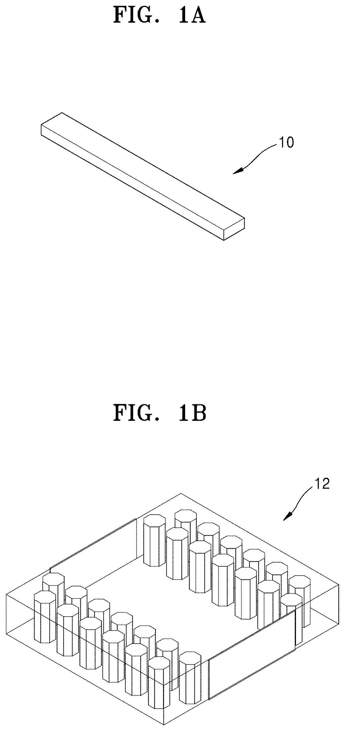
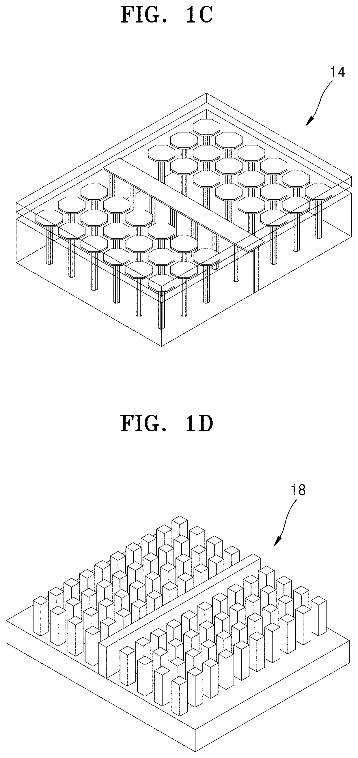
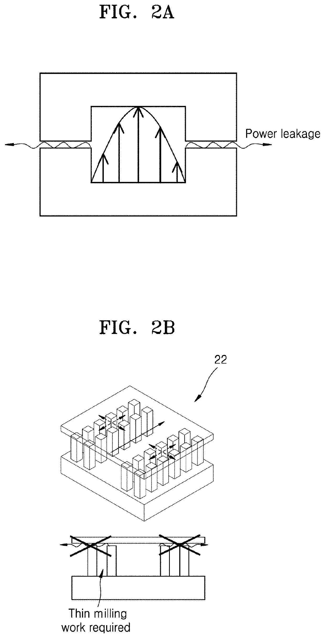
[0061]Embodiments of the disclosure will be described in detail with reference to the accompanying drawings. In the drawings, like reference numerals may denote like elements, and the size of each element may be exaggerated convenience of description. In addition, descriptions of well-known functions and constructions may be omitted for the sake of clarity and conciseness.

[0062]Terms such as “first”, “second”, and “third” may be used herein to describe various elements, components, regions, layers, and / or sections which should not be limited by these terms. These terms are only used to distinguish one element, component, region, layer, or section from another element, component, region, layer, or section. Thus, a first element, component, region, layer, or section may be referred to as a second element, component, region, layer, or section without departing from the scope of the disclosure. As used herein, the expression “and / or” includes any and all combinations of one or more of t...


PUM

PropertyMeasurementUnit
operating frequencyaaaaaaaaaa
insertion lossaaaaaaaaaa

Abstract

Disclosed is a ridge guide waveguide including a conductive base, a conductive ridge protruding upward from the conductive base and extending along a predetermined wave transmission direction, an upper conductive wall located over the conductive base and the conductive ridge and spaced apart from the conductive ridge by a gap, and an electromagnetic bandgap structure arranged adjacent to the conductive ridge between the conductive base and the upper conductive wall.

Description

CROSS-REFERENCE TO RELATED APPLICATIONS[0001]This application is based on and claims priority under 35 U.S.C. § 119 to Russian Patent Application No. 2018143158, filed on Dec. 6, 2018, in the Russian Patent Office, the entire disclosure of which is incorporated herein by reference.BACKGROUND1. Field[0002]The disclosure relates generally to wireless engineering, and more particularly, to a multilayer millimeter-wave antenna array based on a printed circuit board and a ridge gap waveguide (RGW).2. Description of Related Art[0003]There is an ever-increasing user demand for rapid development of communication technology. Currently, actively developed systems using communication in millimeter-wave bands include data transmission systems operating in 28 gigahertz (GHz) and 60 GHz bands, long-distance wireless power transmission (LWPT) systems operating in fifth generation (5G), wireless gigabit (WiGig), and industrial, scientific, and medical (ISM) 24 GHz bands, and automotive radar system...

Claims


Application Information

Patent Timeline
Patent Type & Authority Applications(United States)
IPC IPC(8): H01P3/12H01P1/20H01Q21/00
CPCH01Q21/0006H01P3/121H01P1/20H01Q21/065H01Q1/38H01Q21/064H01Q1/241H01P3/123H01Q15/006H01P1/2005H01P1/211H01P11/002
Inventor VILENSKIY, ARTEM RUDOLFOVITCHMAKURIN, MIKHAIL NIKOLAEVICHLEE, CHONGMIN
Owner SAMSUNG ELECTRONICS CO LTD
Why Eureka
Try Eureka