Electronic products having embedded porous dielectric, related semiconductor products, and their methods of manufacture

a technology of porous dielectrics and electronic products, applied in the field of integration, can solve the problems of loss of efficiency and/or improper control of functional structures, difficulty in achieving impedance low enough to ensure good impedance matching, etc., and achieve the effect of reducing the footprint required to implement the electro-optical device, reducing the size of the required additional loop, and reducing the optical velocity in the optical waveguid

Pending Publication Date: 2020-11-12
MURATA MFG CO LTD +1
View PDF0 Cites 0 Cited by
  • Summary
  • Abstract
  • Description
  • Claims
  • Application Information

AI Technical Summary

Benefits of technology

[0012]Firstly, by suitable adjustment of the porosity ratio of the porous layer, the apparent permittivity εeff of the medium may be controlled. Control of εeff enables control of the velocity factor Vf which is correlated to the velocity of the electrical signal in the electrical transmission line. A desired velocity of the electrical signal in the electrical transmission line, to meet particular application requirements for example, can thus be achieved.
[0045]According to the above method, the porosity ratio achieved in the dielectric underlying the conductors of the electrical transmission line, and hence the effective permittivity, can be controlled in a simple manner by control of the anodization process that anodizes the metal layer.

Problems solved by technology

Indeed, improper impedance matching can result in a large fraction of the electrical wave being reflected back to the source, resulting in loss of efficiency and / or improper control of the functional structure.
However, in practice, using conventional dielectrics it is difficult to achieve an impedance low enough to assure good impedance matching because the minimum dimensions (critical dimensions, CDs) achievable with conventional technologies (e.g. co-fired ceramics) are limited to several dozens of μm for line width / space within a plane and for the diameter / pitch of a connecting via-hole conductor.

Method used


Image

  • Electronic products having embedded porous dielectric, related semiconductor products, and their methods of manufacture
  • Electronic products having embedded porous dielectric, related semiconductor products, and their methods of manufacture
  • Electronic products having embedded porous dielectric, related semiconductor products, and their methods of manufacture

Examples


Embodiment Construction

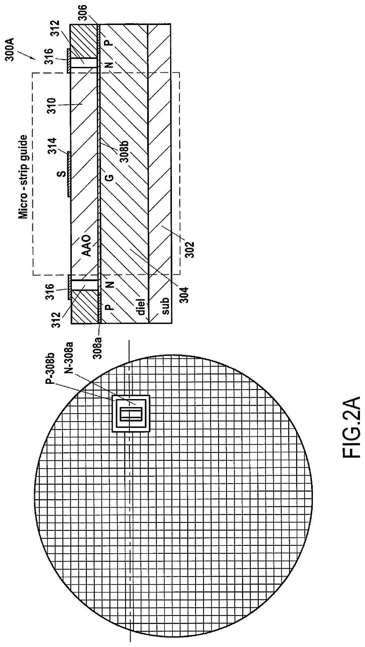
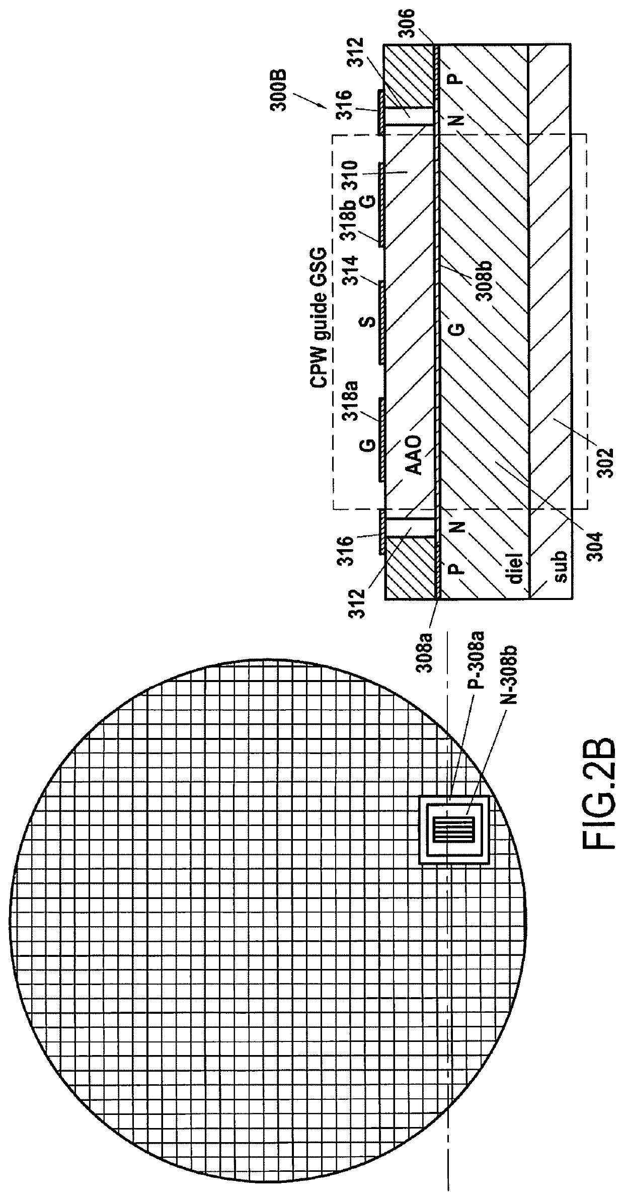
[0062]FIG. 2A illustrates a top view and a cross-section view of an example electronic product 300A according to an embodiment. (Likewise, FIGS. 2B and 2C below also show top views and cross-section views of electronic products). As shown in FIG. 2A, electronic product 300A includes a silicon-on-insulator (SOI) substrate formed of a silicon base substrate 302, an insulator layer 304 formed on the base substrate 302, and a thin silicon layer 306 formed on the insulator layer 304. In an embodiment, the insulator layer 304 is a buried oxide layer made of 902, and the thin silicon layer 306 is a p-type silicon layer having relatively low doping (for example, doping with boron at a concentration of 1×10¹⁷ a / cm3).

[0063]Regions 308a and 308b having specified doping types and levels are formed in the thin silicon layer 306. In an embodiment, region 308b is a region of relatively light n-type doping, and region 308a is a region of relatively light p-type doping. A PN diode is formed by the r...


PUM

PropertyMeasurementUnit
porosity ratioaaaaaaaaaa

Abstract

An electronic product having a silicon-on-insulator substrate, a porous layer of anodic oxide or anodic hydroxide over the silicon layer of the silicon-on-insulator substrate, and a metal layer over the porous layer and that defines at least one electrical transmission line. The velocity of the electrical signal in the at least one electrical transmission line may be controlled by appropriate configuration of the porosity ratio of the porous layer.

Description

CROSS REFERENCE TO RELATED APPLICATIONS[0001]The present application is a continuation of International application No. PCT / EP2019 / 051485, filed Jan. 22, 2019, which claims priority to European Patent Application No. 18305056.6, filed Jan. 25, 2018, the entire contents of each of which are incorporated herein by reference.FIELD OF THE INVENTION[0002]The present invention relates to the field of integration and, more particularly, to electronic products, related semiconductor products, and their methods of manufacture.BACKGROUND OF THE INVENTION[0003]In recent years semiconductor products have been developed in which different electrical sub-blocks are integrated on a common substrate in order to build functions to generate, transmit, convert, detect, etc. electrical signals. Many advanced chips need to couple electronic functions to additional electronic functions or components either on the same substrate or by stacking according to packaging solutions.[0004]FIG. 1 shows a plan vie...

Claims


Application Information

Patent Timeline
Patent Type & Authority Applications(United States)
IPC IPC(8): G02F1/225H01L27/12H01L23/528H01L23/522
CPCG02F1/2257G02F1/2255H01L27/1203H01L23/528G02F2001/212H01L23/5226G02B6/131H01L23/48H01L23/522H01L29/786G02B2006/12061G02F1/212
Inventor VOIRON, FRÉDÉRICEL SABAHY, JULIENFOURNEAUD, LUDOVIC
Owner MURATA MFG CO LTD
Why Eureka
Try Eureka