Method for Selective Delamination and Transfer of Thin Film Using Liquid Platform

a technology of liquid platform and thin film, applied in the field of selective delamination and transfer, can solve the problems of low thermal stability of materials, limited pattern resolution to 100 nanometers (nm), and difficult application of vapor deposition methods, so as to avoid chemical damage and environmental contamination problems, and facilitate the transfer of thin films.

Active Publication Date: 2020-12-10
KOREA ADVANCED INST OF SCI & TECH
View PDF0 Cites 1 Cited by
  • Summary
  • Abstract
  • Description
  • Claims
  • Application Information

AI Technical Summary

Benefits of technology

[0024]According to some example embodiment, there may be provided a method of delaminating an interface between a substrate and a thin film using a surface tension of a liquid material and a method of easily transferring a thin film of a desired pattern or a desired region by inducing a selective change in a wettability of a thin film material through surface treatment. Through this, it is possible to achieve a patterning process having a resolution beyond limitations found in existing processes. For example, a pattern size or a linear width may be widely controllable ranging from a centimeter scale to a nanometer scale.
[0025]Also, according to some example embodiments, there may be provided a selective transfer method that is easily applicable to biotechnology and eco-friendly since an etching process is not required and light is not directly exposed to a substrate. The use of etchant may cause chemical damage to a thin film and a substrate and may also cause a chemical waste treatment issue and accordingly, may be avoided.
[0026]Also, according to some example embodiments, patterning and transfer may be performed using only a liquid material, generally, for example, water, without using etchant. Therefore, it is possible to provide technology very suitable for the current trend, avoiding from chemical damage and environmental contamination issues.
[0027]According to some example embodiments, there may be provided a contact free thin film pattern formation method that may perform a highly efficient process at a low cost. In the existing photolithography and soft lithography methods for forming a pattern of a thin film, the photolithography method uses a non-contact type, however, requires a high cost and high technical equipment and clean room environment. The soft lithography method may perform a relatively low cost and high throughput process, however, may cause a postprocessing issue due to a contamination material and micro particles on the surface since a contact-type process is used. The present disclosure may be employed as an alternative to outperform the aforementioned issues and may readily perform a next-generation electronic product manufacture even in a small scale laboratory.

Problems solved by technology

Here, since a polymer material has a low thermal stability, a vapor deposition method, such as a physical vapor deposition (PVD) method and a chemical vapor deposition (CVD) method, may not be readily applied.
However, in the photolithography method, a patternable resolution is limited to 100 nanometers (nm) or more due to an optical diffraction phenomenon and a relatively large cost is required due to the complexity of a process and equipment.
Also, the photolithography method may have a chemical waste occurrence issue caused by the use of etchant and a chemical damage issue unintendedly caused in a thin film.
Further, it is difficult to apply a patterning process on a curved surface.
However, still expensive equipment is required, which makes it difficult for general researchers to readily employ the technique.
However, the soft lithography method may have the following limitations.
First, due to the relatively high flexibility and deformability of an elastomeric stamp, unexpected deformation, for example lateral collapse and sagging of the patterned stamp, may occur and it may be difficult to achieve a relatively high resolution.
Accordingly, it may be difficult to accurately embody a detailed pattern.
Second, a contact scheme may cause an issue in other processes followed by a lithographic process due to a contamination material and a microparticle, etc., on the surface.
However, they are still at a technically low stage to be commercially available due to limitations, for example, a process resolution, application of various thin film materials, and a thickness minimization.
In the existing photolithography and soft lithography methods for forming a pattern of a thin film, the photolithography method uses a non-contact type, however, requires a high cost and high technical equipment and clean room environment.
The soft lithography method may perform a relatively low cost and high throughput process, however, may cause a postprocessing issue due to a contamination material and micro particles on the surface since a contact-type process is used.

Method used


Image

  • Method for Selective Delamination and Transfer of Thin Film Using Liquid Platform
  • Method for Selective Delamination and Transfer of Thin Film Using Liquid Platform
  • Method for Selective Delamination and Transfer of Thin Film Using Liquid Platform

Examples


Embodiment Construction

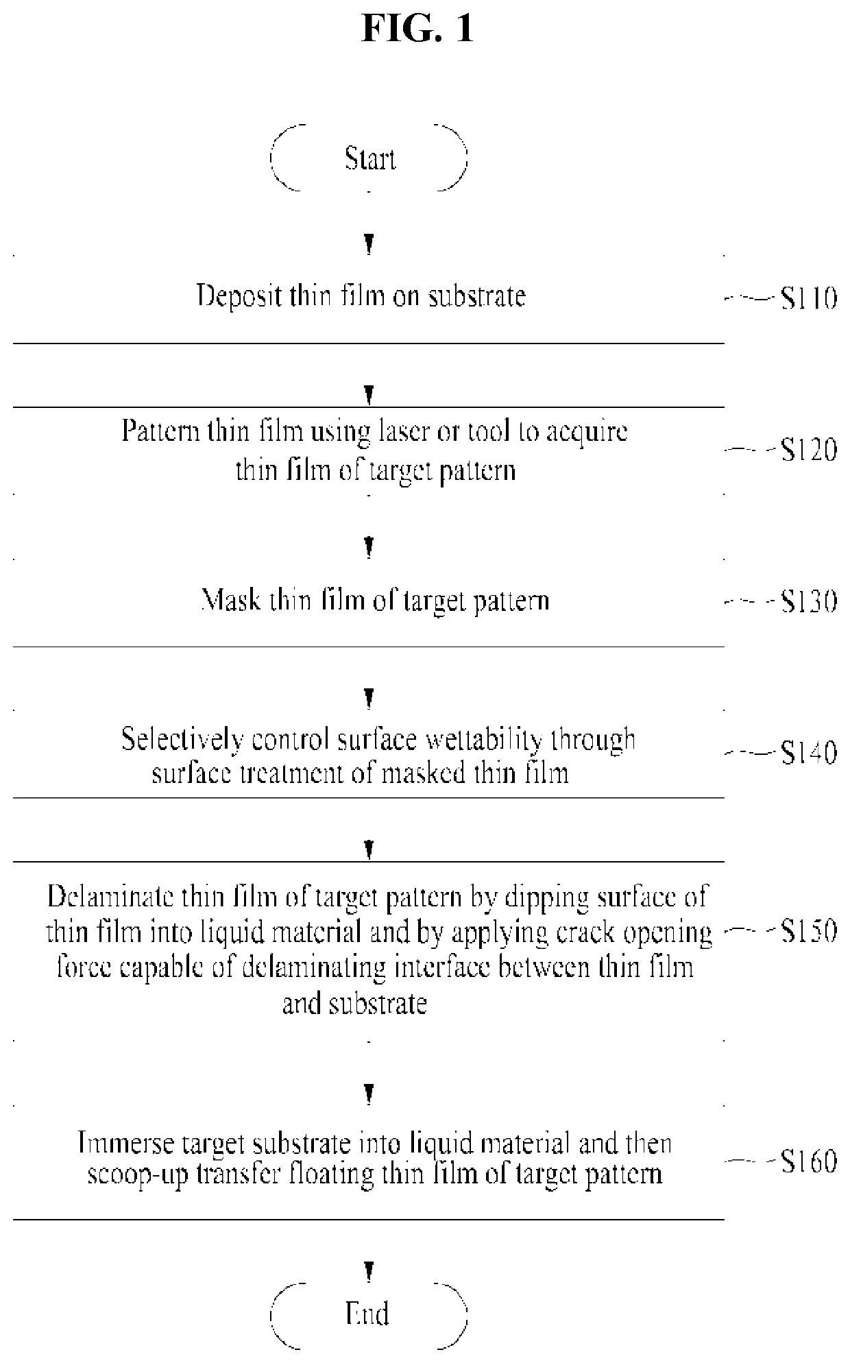
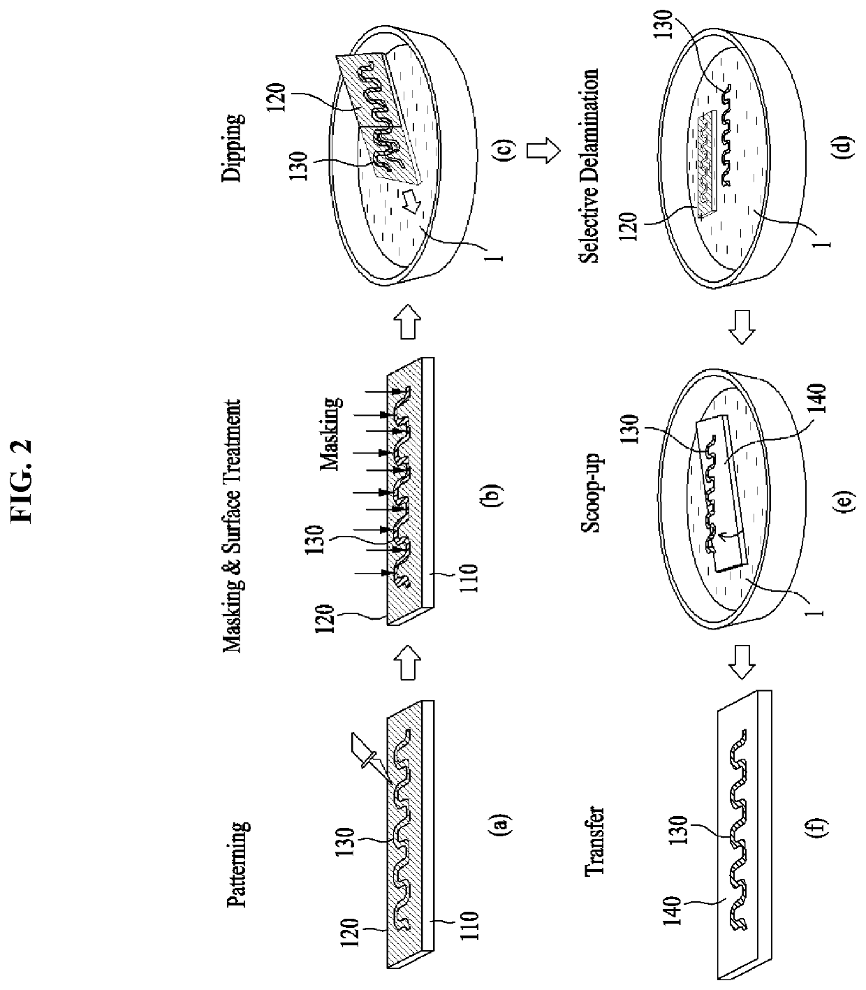
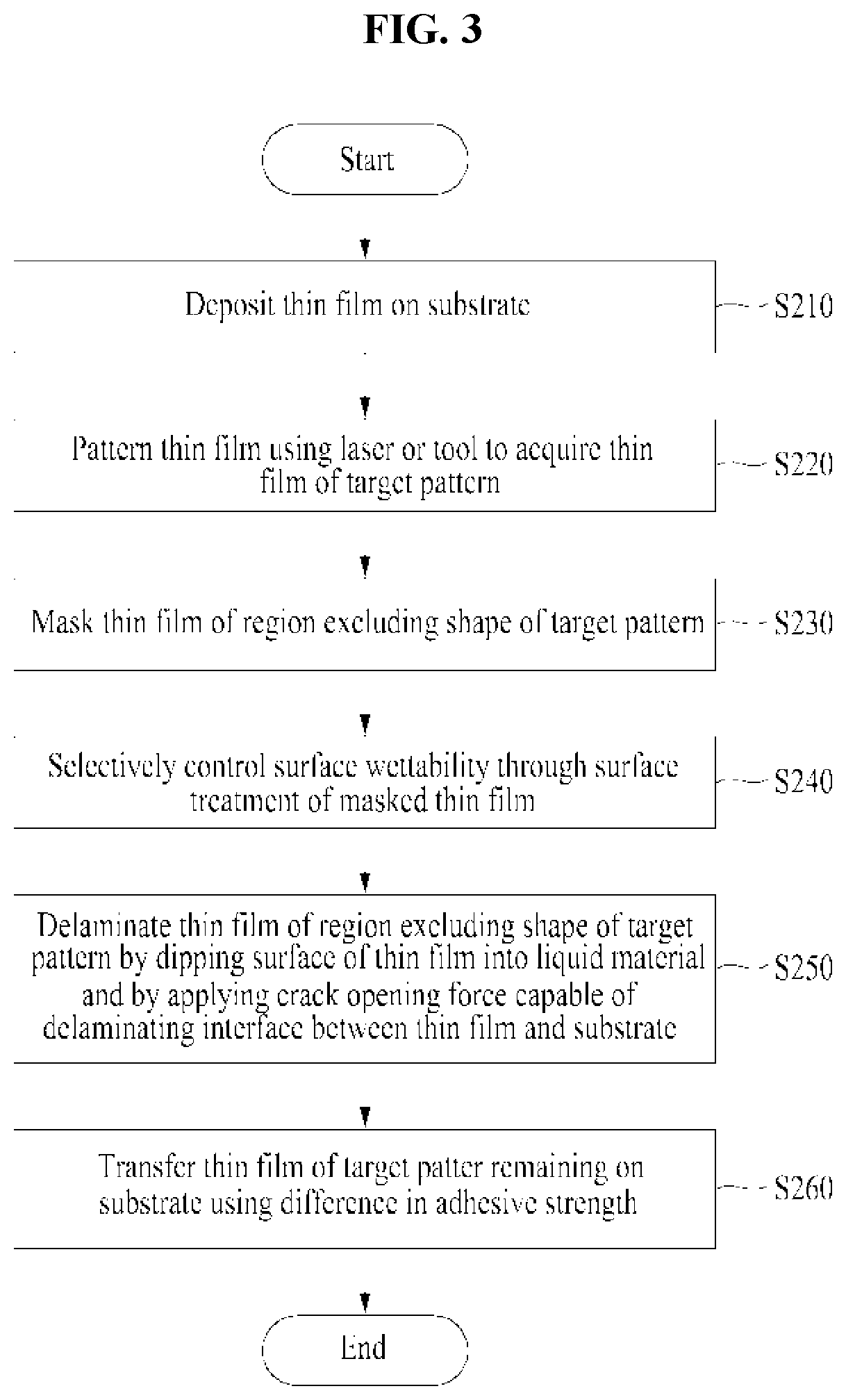
[0042]One or more example embodiments will be described in detail with reference to the accompanying drawings. Example embodiments, however, may be embodied in various different forms, and should not be construed as being limited to only the illustrated embodiments. Rather, the illustrated embodiments are provided as examples so that this disclosure will be thorough and complete, and will fully convey the concepts of this disclosure to those skilled in the art. Accordingly, known processes, elements, and techniques, may not be described with respect to some example embodiments.

[0043]When a component is described to be on another component, the component may be directly formed on the other component or a third component may be provided between the components. Also, in the drawings, thicknesses of components may be exaggerated to effectively describe technical content. Unless otherwise noted, like reference numerals refer to like components throughout the attached drawings and written...


PUM

PropertyMeasurementUnit
thicknessaaaaaaaaaa
surface wettabilityaaaaaaaaaa
wettabilityaaaaaaaaaa

Abstract

Provided is a selective transfer method including depositing a thin film on a substrate; patterning the thin film using a laser or a tool to acquire a thin film of a target pattern; masking the thin film of the target pattern; selectively controlling a surface wettability through surface treatment of the masked thin film; delaminating the thin film of the target pattern by dipping a surface of the thin film with a wettability changed in response to a completion of the selective surface treatment into a liquid material and by applying a crack opening force capable of delaminating an interface between the thin film and the substrate; and immersing a target substrate into the liquid material when the thin film of the target pattern is floating in the liquid material and then scoop-up transferring the floating thin film of the target pattern.

Description

[0001]This application claims the priority benefit of Korean Patent Applications No. 10-2019-0067201, filed on Jun. 7, 2019 and No. 10-2019-0142449, filed on Nov. 8, 2019, in the Korean Intellectual Property Office, the disclosure of which is incorporated herein by reference.BACKGROUND1. Field of the Invention[0002]The following description of example embodiments relates to a selective delamination and transfer method, and more particularly, to a method of selectively delaminating and transferring a thin film of a desired pattern or a thin film of a desired region using a liquid platform.2. Description of the Related Art[0003]Currently, research on using a thin film and a two-dimensional material having mechanically, electrically, and optically excellent performance for, for example, wearable, flexible, and stretchable electronic devices, semiconductor devices, and wireless communication devices, is conducted. To develop and commercialize such application products, there is a need t...

Claims


Application Information

Patent Timeline
Patent Type & Authority Applications(United States)
IPC IPC(8): G03F7/20H01L29/786
CPCG03F7/2043H01L29/78603G03F7/2002G03F7/70025B32B37/025C10G2/32B44C1/175C10G2300/70
Inventor KIM, TAEK-SOOKANG, SUMIN
Owner KOREA ADVANCED INST OF SCI & TECH
Why Eureka
Try Eureka