Silicon carbide semiconductor device

Active Publication Date: 2020-12-10
MITSUBISHI ELECTRIC CORP
View PDF0 Cites 3 Cited by
  • Summary
  • Abstract
  • Description
  • Claims
  • Application Information

AI Technical Summary

Benefits of technology

The invention forms a capacitance in a silicon carbide semiconductor device by creating a low-resistance region in the second trench through the insulation film. This allows for a larger displacement current to pass through the second relaxation region below the second trench and branch into the low-resistance region through capacitive coupling, resulting in a reduction in potential drop.

Problems solved by technology

As a result, intolerably large potential drop may occur in the p-type wells.
This may raise concern about occurrence of dielectric breakdown due to the potential difference.
In addition, it is more difficult to perform treatment of reducing electric resistance by means of doping on silicon carbide than silicon.
Thus, when silicon carbide is used, the p-type well is liable to have large parasitic resistance.
Such large parasitic resistance may easily lead to large potential drop in the p-type well.

Method used


Image

  • Silicon carbide semiconductor device
  • Silicon carbide semiconductor device
  • Silicon carbide semiconductor device

Examples


first embodiment

[0036](Configuration)

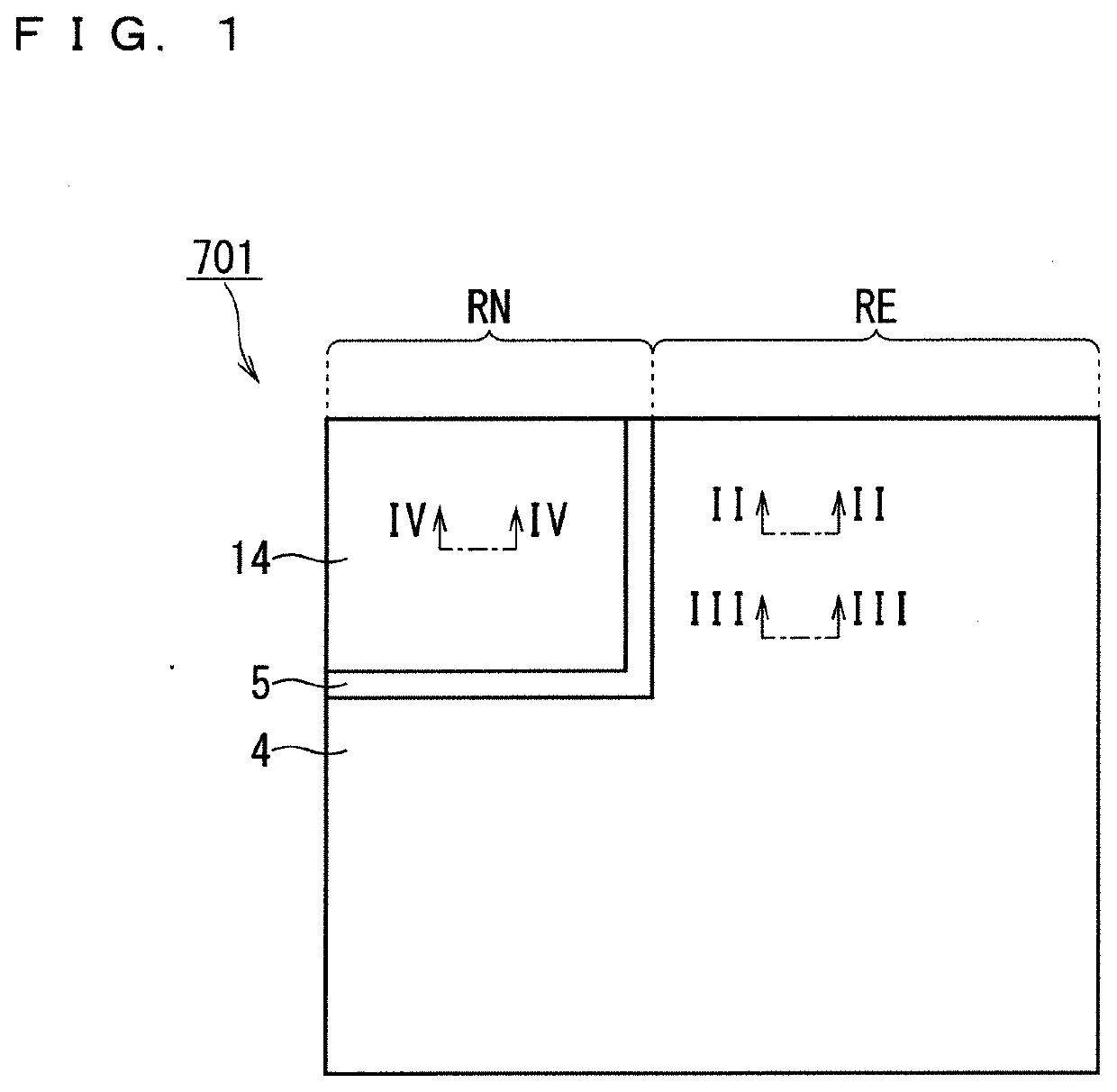
[0037]FIG. 1 is a plan view schematically illustrating a configuration of a MOSFET 701 (silicon carbide semiconductor device) according to the first embodiment. The MOSFET 701 includes an element region RE provided on a substrate 11 (silicon carbide semiconductor substrate) and a non-element region RN provided outside the element region RE. In the MOSFET 701, a gate pad electrode 14 connected to the outside and supplied with a gate voltage from the outside is disposed in the non-element region RN. A wire made of metal such as aluminum is connected to the gate pad electrode 14 by means of ultrasonic joining or the like. The non-element region RN may include a termination region of the MOSFET 701. The element region RE includes a region in which channels controlled by gate electrodes are disposed, and typically is a region in which a MOSFET cell that actually functions as a MOSFET is disposed.

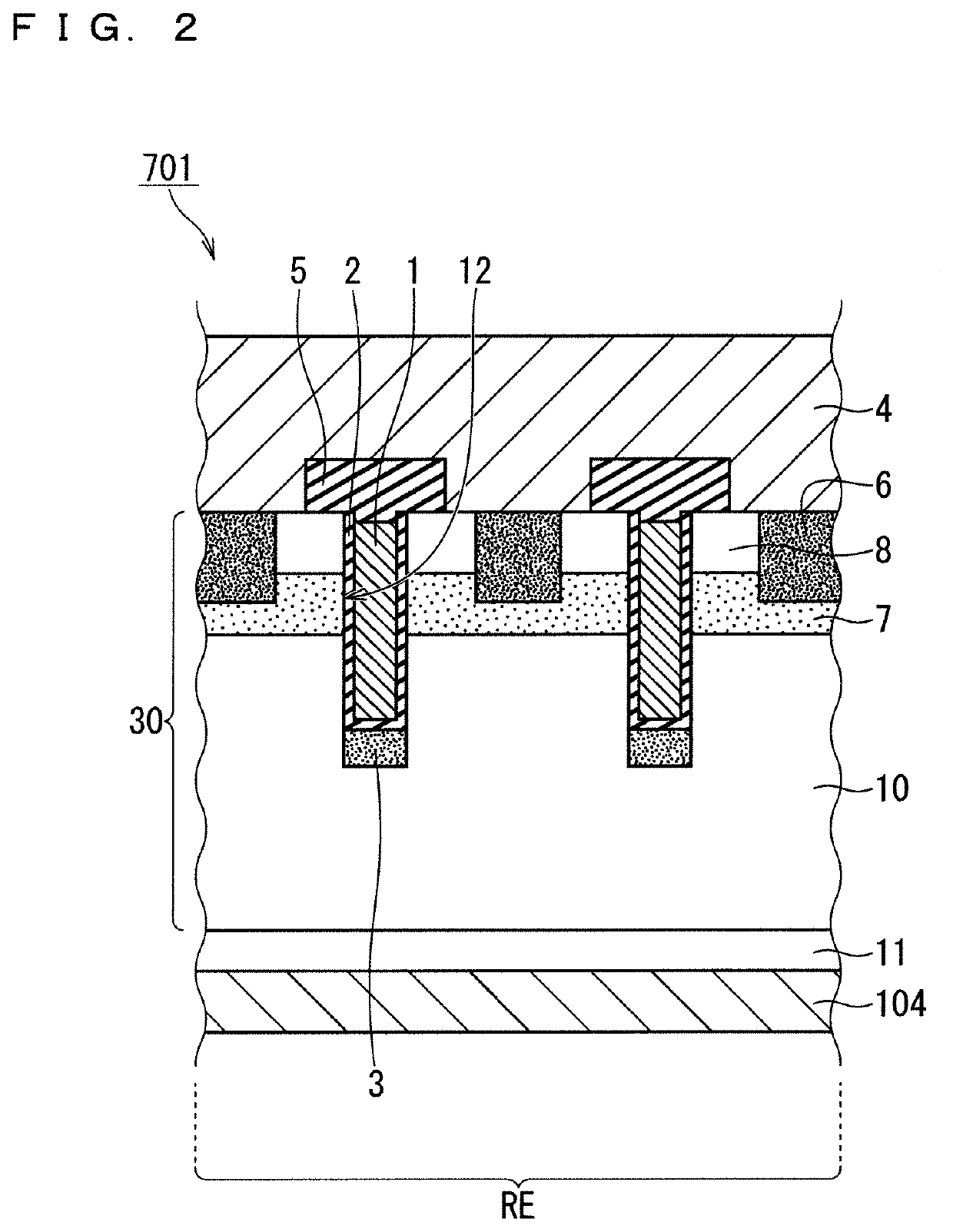
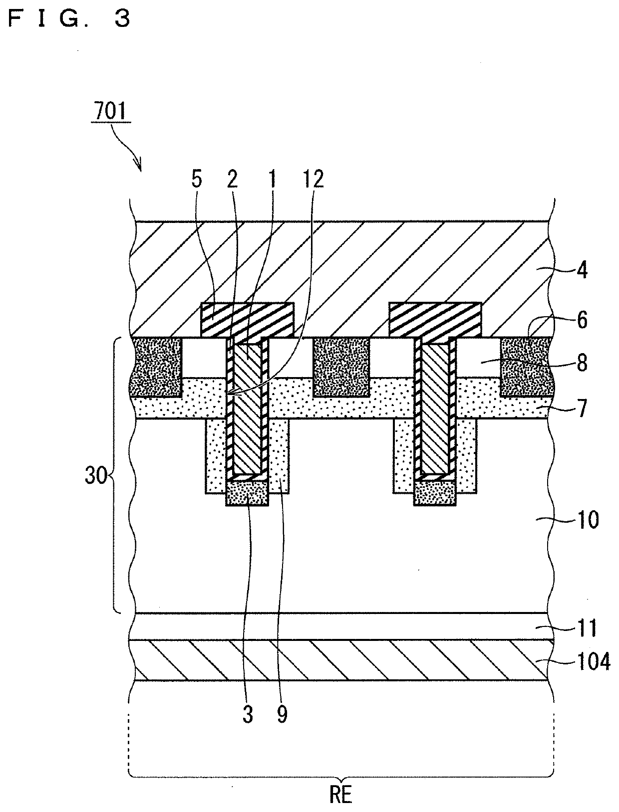
[0038]FIG. 2 and FIG. 3 schematically illustrate different partial cross...

second embodiment

[0063]FIG. 7 is a plan view schematically illustrating a configuration of a MOSFET 702 (silicon carbide semiconductor device) according to the second embodiment. In plan view, the MOSFET 702 includes a contact region RC between the element region RE and the non-element region RN.

[0064]FIG. 8 is a schematic partial cross-sectional view taken along the line VIII-VIII of FIG. 7. In the contact region RC, a drift layer 10 having the n type (first conductivity type) provided on the substrate 11, a third trench 212 whose bottom surface reaches the drift layer 10, and a third relaxation region 203 are provided. In the present embodiment, the third trench 212 is provided in the epitaxial layer 30 in at least a part of the contact region RC. The third trench 212 includes a side surface and a bottom surface. The third trench 212 may have depth the same as the depth of the first trench 12.

[0065]The MOSFET 702 includes a third relaxation region 203 disposed in the contact region RC. Specificall...

third embodiment

[0072]FIG. 9 is a partial cross-sectional view of a configuration of a MOSFET 703 (silicon carbide semiconductor device) according to the third embodiment, which is illustrated in a cross-section similar to that taken along the line VIII-VIII of FIG. 7. In plan view (see FIG. 7), between the element region RE and the non-element region RN, the MOSFET 703 includes a contact region RC in which a part of the low-resistance region 101 (FIG. 9) is disposed. In the configuration of FIG. 9, the low-resistance region 101 has a part disposed in the third trench 212 that is provided in the contact region RC, and this part is connected to a part of the low-resistance region 101 disposed in the second trench 112. In the contact region RC, the low-resistance region 101 and the source pad electrode 4 are electrically connected. In order to achieve this electrical connection, typically, in the contact region RC, the source pad electrode 4 includes a contact 216 that extends in the inter-layer insu...


PUM


Abstract

In an element region and a non-element region, a silicon carbide semiconductor device includes a drift layer having a first conductivity type provided on a silicon carbide semiconductor substrate. In the element region, the silicon carbide semiconductor device includes a first trench that reaches the drift layer, and a gate electrode provided in the first trench through a gate insulation film and electrically connected to a gate pad electrode. In the non-element region, the silicon carbide semiconductor device includes a second trench whose bottom surface reaches the drift layer, a second relaxation region having a second conductivity type disposed below the second trench, an inner-surface insulation film provided on a side surface and on the bottom surface of the second trench, and a low-resistance region provided in the second trench through the inner-surface insulation film and electrically insulated from the gate pad electrode.

Description

TECHNICAL FIELD[0001]The present invention relates to a silicon carbide semiconductor device.BACKGROUND ART[0002]As a switching element used in an inverter circuit or the like, a vertical power semiconductor device is widely used, and particularly a vertical power semiconductor device having a metal-oxide-semiconductor (MOS) structure is widely used. Typically, an insulated gate bipolar transistor (IGBT) and a metal-oxide-semiconductor field-effect transistor (MOSFET) are used. For example, WO 2010 / 098294 (Patent Document 1) discloses a MOSFET, and Japanese Patent Application Laid-Open No. 2004-273647 (Patent Document 2) discloses an IGBT. Patent Document 1 particularly discloses a vertical n-channel MOSFET that uses silicon carbide (SiC) as a semiconductor material. Further, WO 2012 / 077617 (Patent Document 3) discloses a trench-gate MOSFET, with the aim of further reducing an on-voltage of a vertical n-channel MOSFET using silicon carbide.[0003]The n-channel MOSFET includes an n-ty...

Claims


Application Information

Patent Timeline
IPC IPC(8): H01L29/78H01L29/16H01L29/40H01L29/10
CPCH01L29/407H01L29/404H01L29/1045H01L29/1083H01L29/7813H01L29/1608H01L29/0623H01L29/1095H01L29/0696H01L29/7805H01L29/7811
Inventor TOMINAGA, TAKAAKI
Owner MITSUBISHI ELECTRIC CORP
Why Eureka
Try Eureka