Eureka AIR delivers breakthrough ideas for toughest innovation challenges, trusted by R&D personnel around the world.

Optical modulator

Inactive Publication Date: 2021-01-28
SUMITOMO OSAKA CEMENT CO LTD
View PDF0 Cites 0 Cited by
  • Summary
  • Abstract
  • Description
  • Claims
  • Application Information

AI Technical Summary

Benefits of technology

The present invention relates to an optical modulator that uses a substrate with an electro-optic effect to modulate light waves. The invention provides a thinner substrate and a reinforcing substrate that holds the substrate through an adhesive layer. The adhesive layer includes an air gap section where no adhesive agent is present, which results in a thinner adhesive layer and improved performance. The invention overcomes the limitations associated with thick adhesive layers that decrease adhesive strength, increase stress, and decrease yield during chip cutting.

Problems solved by technology

However, in this configuration, since an electric field applied to the optical waveguide decreases due to the presence of the buffer layer, there is a problem that voltage reduction of a drive voltage may not be realized.
In a case in which the thickness of the adhesive layer is increased as described above, firstly, there is a problem that the adhesive strength is decreased.
Secondly, in a case in which the temperature of the adhesive agent increases due to ultraviolet irradiation or heating during curing, and the temperature decreases after the adhesive agent is cured, stress due to a difference in linear expansion coefficient between the adhesive agent (adhesive layer) and the optical waveguide substrate or reinforcing substrate is generated.
Thus, as the adhesive layer is thick, the stress is also large.
Thirdly, it is difficult to cut an adhesive layer formed thick into chips, so that a yield is decreased.

Method used


Image

  • Optical modulator

Examples


Embodiment Construction

[0021]Hereinafter, the optical modulator of the present invention will be described in detail with reference to suitable examples.

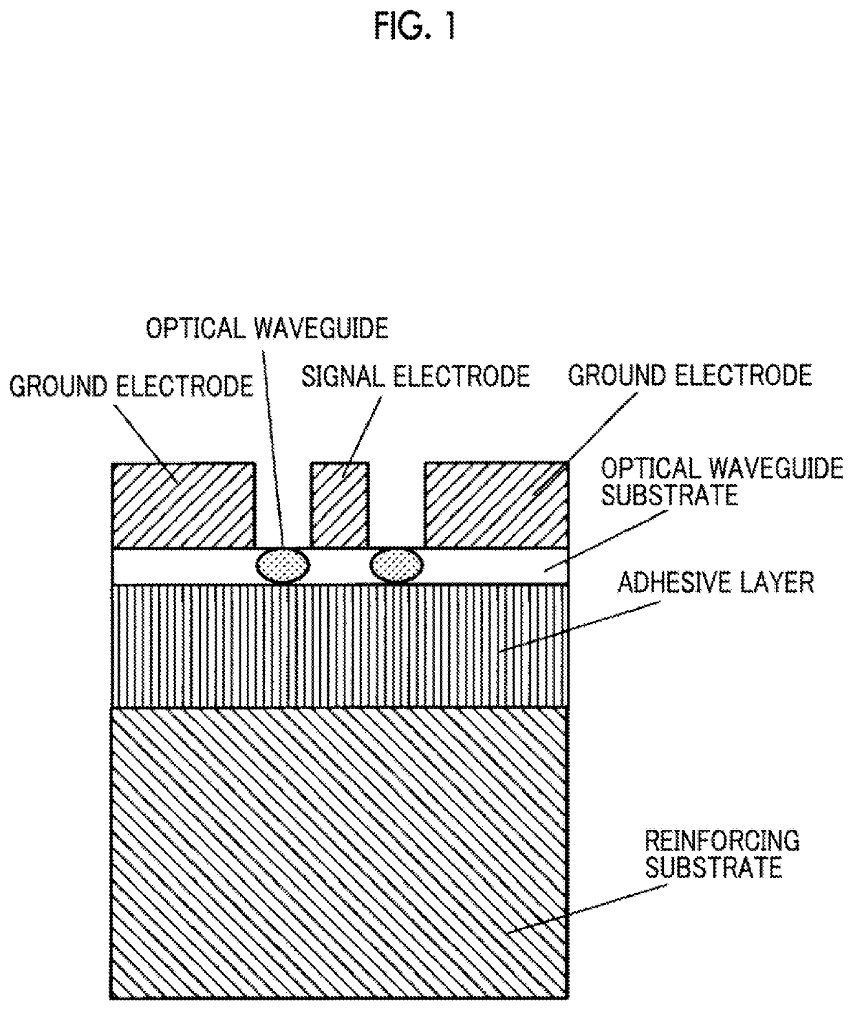
[0022]In the present invention, as shown in FIG. 1, the optical modulator includes features as follows: a substrate (optical waveguide substrate) having an electro-optic effect; an optical waveguide formed on the substrate; and a traveling-wave electrode (signal electrode and ground electrode) formed on the substrate in order to modulate a light wave propagating through the optical waveguide, in which the substrate has a thickness of 30 μm or lower, a reinforcing substrate that holds the substrate through an adhesive layer interposed between the reinforcing substrate and the substrate is provided, and the adhesive layer includes an air gap section where no adhesive agent is present. In addition, a proportion of the air gap section to an entirety of the adhesive layer is 25% by volume to 60% by volume.

[0023]As the optical waveguide substrate, a substrate f...


PUM


Abstract

Provided is an optical modulator that includes an adhesive layer whose thickness can be reduced and that ensures high reliability, while band-widening and low voltage drive are realized.An optical modulator includes features as follows: a substrate (optical waveguide substrate) having an electro-optic effect; an optical waveguide formed on the substrate; and a traveling-wave electrode (signal electrode and ground electrode) formed on the substrate in order to modulate a light wave propagating through the optical waveguide, in which the substrate has a thickness of 30 μm or lower, a reinforcing substrate that holds the substrate through an adhesive layer interposed between the reinforcing substrate and the substrate is provided, and the adhesive layer includes an air gap section where no adhesive agent is present.

Description

TECHNICAL FIELD[0001]The present invention relates to an optical modulator, and particularly, relates to an optical modulator in which a substrate having an electro-optic effect and a thickness of 30 μm or lower is used.BACKGROUND ART[0002]In recent years, higher speed and capacity of an optical communication system have been progressing, and for example, an optical communication system having a communication speed of 100 GHz or higher per one wavelength has been considered practical. From now on, band-widening of the optical modulator, which is a basic component, will be much more demanded.[0003]A traveling-wave optical modulator causes light waves propagating through an optical waveguide and microwaves propagating through an electrode (traveling-wave electrode) provided along the optical waveguide to interact with each other due to an electro-optic effect, thereby modulating the light wave. In particular, band-widening can be realized by achieving velocity matching of the light wa...

Claims


Application Information

Patent Timeline
IPC IPC(8): G02F1/035
CPCG02F1/0356G02F2202/28G02F2201/127G02F1/035
Inventor KUGIMOTO, YUKIHOSOKAWA, YOICHI
Owner SUMITOMO OSAKA CEMENT CO LTD
Why Eureka
Eureka Blog
Learn More