Eureka AIR delivers breakthrough ideas for toughest innovation challenges, trusted by R&D personnel around the world.

Insulating film material, multilayer interconnection structure, method for manufacturing same, and method for manufacturing semiconductor device

Inactive Publication Date: 2008-08-28
FUJITSU LTD
View PDF5 Cites 10 Cited by
  • Summary
  • Abstract
  • Description
  • Claims
  • Application Information

AI Technical Summary

Benefits of technology

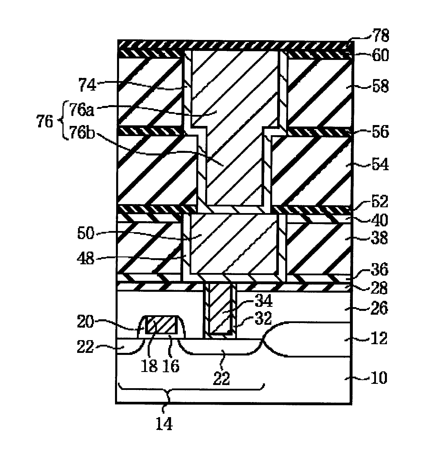
[0013]The insulating film material contains a silicon compound having a steric structure represented by the Structural Formula (1), and in this steric structure, bonds of silicon atoms and carbon atoms (Si—R—Si bonds, where R is a functional group represented by the R1 to R4 above) are regularly bonded via oxygen atoms. As a result, voids are formed in the skeleton of the steric structure and a dielectric constant is decreased. Further, because rigid Si—R—Si bonds are contained, the degree of freedom of the bonds is small, and an insulating film formed using the insulating film material has a high strength and excels in resistance to damage, such as etching resistance and resistance to liquid reagents. Therefore, the insulating film material can be advantageously used for forming an insulating film and a multilayer interconnection structure, can be advantageously used for manufacturing semiconductor devices of various kinds and can be especially advantageously used for manufacturing the multilayer interconnection structure of an aspect of an embodiment.
[0014]A signal propagation speed has been known to be decreased by a parasitic capacitance of insulating films, but in the generation of semiconductor devices with an interconnection spacing of 1 μm or more, the effect of the interconnection delay on the entire device is small. The degree of integration of semiconductor integrated circuits has recently increased and a transition was made to multilayer interconnection structures which resulted in decreased interconnection width and spacing. Thus, where a circuit is formed with an interconnection spacing of 1 μm or less, and especially 0.1 μm or less, as will be in the future circuits, the parasitic capacitance between interconnections produces a significant effect on the device speed.
[0015]Presently, a multilayer interconnection structure of a semiconductor device is composed of a coating-type insulating film with a low dielectric constant, an etching stopper film formed by plasma CVD, and a diffusion barrier insulating film, but the coating-type insulating film with a low dielectric constant is most often produced as a porous film to meet the requirement relating to the decrease in dielectric constant, and such film is easily damaged by processing during multilayer interconnection structure formation. Therefore, the resistance to damage has to be increased. Further, at present, multilayer interconnection structures and semiconductor devices are manufactured by processing the film with a low dielectric constant by plasma, electron beam, liquid reagents, and the like, and each of these methods can cause an increase in dielectric constant due to damage of the film with a low dielectric constant. However, the insulating film formed from the insulating film material of an aspect of an embodiment has a low dielectric constant, excels in damage resistance, and can contribute to the increase in response speed. Therefore, the decrease in parasitic capacitance between the interconnections can be attained and the signal propagation speed can be increased.
[0017]Because the multilayer interconnection structure has an interlayer insulating film that is formed using the insulating film material of an aspect of an embodiment, has a lower dielectric constant and reduced parasitic capacitance and also excels in resistance to damage, the signal propagation speed can be increased. Such a multilayer interconnection structure is especially suitable, for example, to semiconductor integrated circuits with a high degree of integration such as IC and LSI that require increase in the response speed.
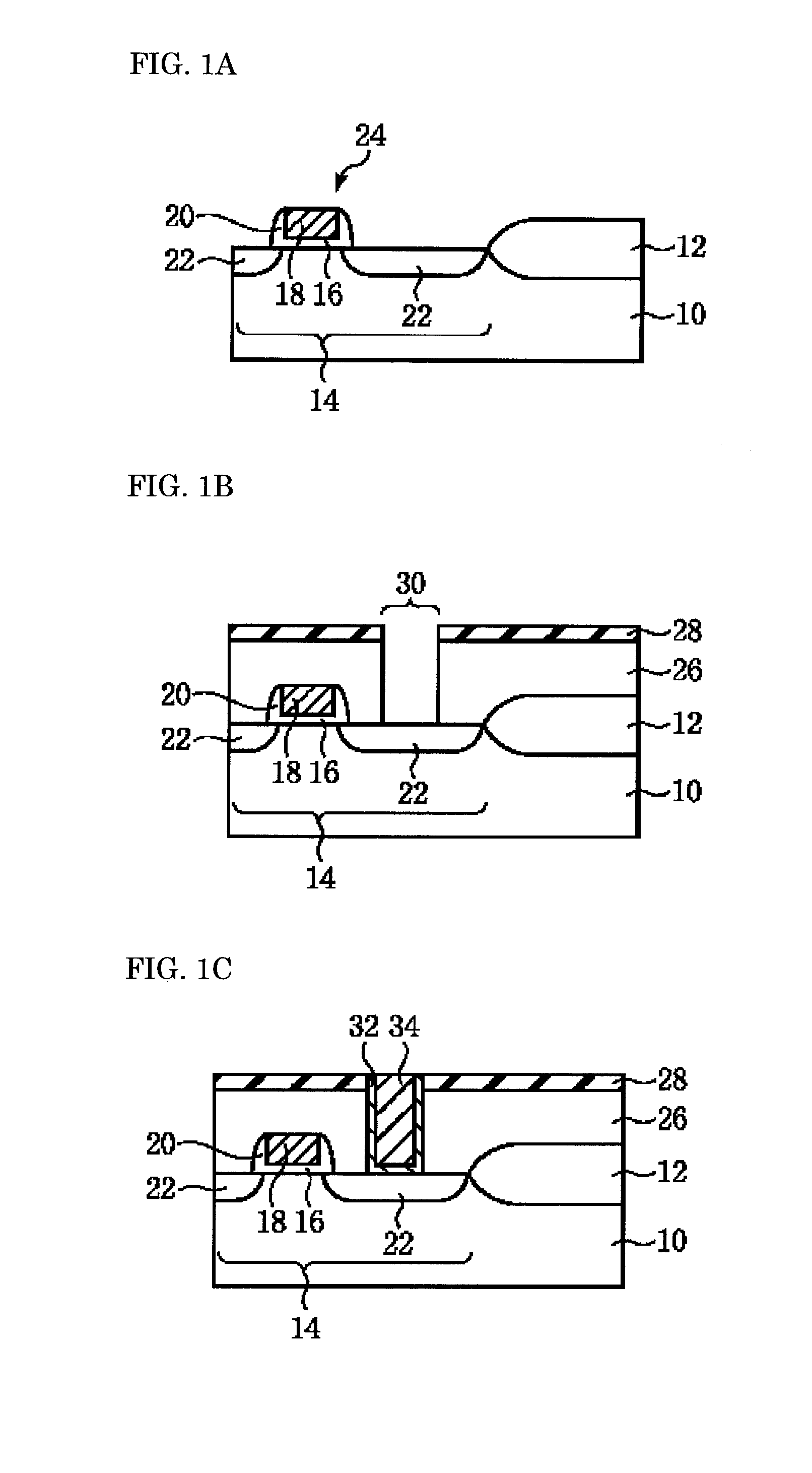
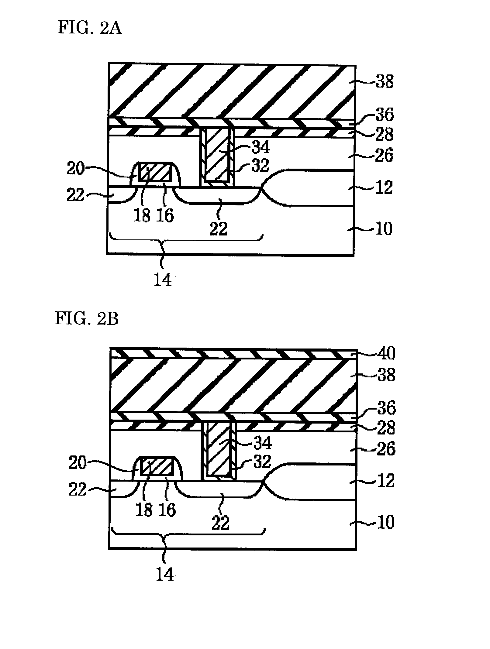
[0021]In the method for manufacturing a semiconductor device, a multilayer interconnection structure is formed on the surface to be processed by the method for manufacturing the multilayer interconnection of an aspect of an embodiment in the step of forming a multilayer interconnection. As a result, the parasitic capacitance between the interconnections can be reduced and interconnection resistance can be decreased, and a high-performance semiconductor device that enables the increase in signal propagation speed can be efficiently manufactured. Such a semiconductor device is especially suitable for flash memories, DRAMs, FRAMs, and MOS transistors.

Problems solved by technology

Because spacing between interconnections further decreases as the degree of integration of semiconductor integrated circuits grows, interconnection delay caused by the increase in capacitance between the interconnections becomes a problem.
Although the capacitance (C) between interconnections can be decreased by reducing the interconnection thickness and decreasing the electrode surface area, the decrease in interconnection thickness causes additional increase in interconnection resistance (R), thereby making it impossible to attain a high speed.
Accordingly, the impedance of metal interconnection determined by electrostatic inductance increases, and the increase in delay of response speed and power consumption causes concerns.
Because porous films have pores, a dielectric constant lower than that in the conventional configurations can be realized, but the problem that is presently associated with this approach is that the pore size is as large as 10 nm or more and where a porosity (pore presence ratio) is increased with the object of further decreasing the dielectric constant, moisture absorption causes increase in dielectric constant and decrease in film strength.
However, at present, multilayer interconnection structures and semiconductor devices are manufactured by processing the films with a low dielectric constant by etching that employs plasma and liquid reagents, and the problem associated with such technique is that dielectric constant increases due to damage to the film with a low dielectric constant.

Method used


Image

  • Insulating film material, multilayer interconnection structure, method for manufacturing same, and method for manufacturing semiconductor device
  • Insulating film material, multilayer interconnection structure, method for manufacturing same, and method for manufacturing semiconductor device
  • Insulating film material, multilayer interconnection structure, method for manufacturing same, and method for manufacturing semiconductor device

Examples


example 1

—Preparation of Insulating Film Material

[0103]A total of 88 g (0.9 mol) of sulfuric acid and 33 g of fuming sulfuric acid (60% SO4) were charged into a reaction container equipped with a nitrogen gas introducing tube and a metering pump for liquids, 87 g (0.95 mol) of toluene was dropwise added under a condition of 2 mL / min with the metering pump, and a maturing reaction was conducted for 1 h after completion of addition.

[0104]Then, a starting material solution obtained by diluting 103 g (0.45 mol) of 1,1,3,3-tetrachloro-1,3-disilabutane to 20% by mass with toluene was dropwise added under a condition of 2 mL / min with the metering pump, and a maturing reaction was conducted for 2 h after completion of addition.

[0105]Upon completion of the reaction, 100 mL of a 50% by mass aqueous solution of sulfuric acid was added, the precipitated toluenesulfonic acid was filtered, and the excessive aqueous sulfuric acid was removed with a separating funnel.

[0106]Sulfuric acid remaining in the so...

example 2

—Preparation of Insulating Film Material

[0111]A total of 88 g (0.9 mol) of sulfuric acid and 33 g of fuming sulfuric acid (60% SO4) were charged into a reaction container equipped with a nitrogen gas introducing tube and a metering pump for liquids, 87 g (0.95 mol) of toluene was dropwise added under a condition of 2 mL / min with the metering pump, and a maturing reaction was conducted for 1 h after completion of dropping.

[0112]Then, a starting material solution obtained by diluting 115 g (0.45 mol) of bis(methyldichlorosilyl)ethane to 20% by mass with toluene was dropwise added under a condition of 2 mL / min with the metering pump, and a maturing reaction was conducted for 2 h after completion of addition.

[0113]Upon completion of the reaction, 100 mL of a 50% by mass aqueous solution of sulfuric acid was added, the precipitated toluenesulfonic acid was filtered, and the excessive aqueous sulfuric acid was removed with a separating funnel.

[0114]Sulfuric acid remaining in the solution...

example 3

—Preparation of Insulating Film Material

[0118]A total of 88 g (0.9 mol) of sulfuric acid and 33 g of fuming sulfuric acid (60% SO4) were charged into a reaction container equipped with a nitrogen gas introducing tube and a metering pump for liquids, 87 g (0.95 mol) of toluene was dropwise added under a condition of 2 mL / min with the metering pump, and a maturing reaction was conducted for 1 h after completion of dropping.

[0119]Then, a starting material solution obtained by diluting 128 g (0.45 mol) of bis(methyldichlorosilyl)butane to 20% by mass with is toluene was dropwise added under a condition of 2 mL / min with the metering pump, and a maturing reaction was conducted for 2 h after completion of dropping.

[0120]Upon completion of the reaction, 100 mL of a 50% by mass aqueous solution of sulfuric acid was added, the precipitated toluenesulfonic acid was filtered, and the excessive aqueous sulfuric acid was removed with a separating funnel.

[0121]Sulfuric acid remaining in the solut...


PUM

PropertyMeasurementUnit
Thicknessaaaaaaaaaa
Thicknessaaaaaaaaaa
Porosityaaaaaaaaaa

Abstract

To provide an insulating film material that can be advantageously used for forming an insulating film having a low dielectric constant and excellent resistance to damage, such as etching resistance and resistance to liquid reagents, a multilayer interconnection structure in which a parasitic capacitance between the interconnections can be reduced, efficient methods for manufacturing the multilayer interconnection structure, and an efficient method for manufacturing a semiconductor device with a high speed and reliability. The insulating film material contains at least a silicon compound having a steric structure represented by Structural Formula (1) below.where, R1, R2, R3, and R4 may be the same or different and at least one of them represents a functional group containing any of a hydrocarbon and an unsaturated hydrocarbon.

Description

CROSS-REFERENCE TO RELATED APPLICATIONS[0001]This application is based upon and claims the benefits of the priority from the prior Japanese Patent Application No. 2007-045762 filed on Feb. 26, 2007, the entire contents of which are incorporated herein by reference.BACKGROUND OF THE INVENTION[0002]1. Field of the Invention[0003]The present invention relates to an insulating film material that can be advantageously used for forming an insulating film within a multilayer interconnection structure in a semiconductor integrated circuit, a multilayer interconnection structure having an insulating film that is formed using the insulating film material and that has a low dielectric constant and excels in resistance to damage, a method for manufacturing the multilayer interconnection structure, and a method for manufacturing a semiconductor device.[0004]2. Description of the Related Art[0005]A demand for multilayer semiconductor elements has recently increased following the increase in the d...

Claims


Application Information

Patent Timeline
IPC IPC(8): H01L23/52H01L21/4763C07F7/08
CPCC09D183/04H01L21/02126H01L2924/0002H01L21/76834H01L21/76829H01L21/02203H01L21/02208H01L21/02282H01L21/3122H01L21/31695H01L21/76801H01L21/76807C08L2666/54H01L2924/00H01L21/02274H01L21/02216C08J5/18C08G77/04C08G77/00H01L21/31
Inventor KOBAYASHI, YASUSHINAKATA, YOSHIHIROOZAKI, SHIROU
Owner FUJITSU LTD
Why Eureka
Eureka Blog
Learn More