Method for manufacturing silicon carbide single crystal
- Summary
- Abstract
- Description
- Claims
- Application Information
AI Technical Summary
Benefits of technology
Problems solved by technology
Method used
Image

Examples
first embodiment
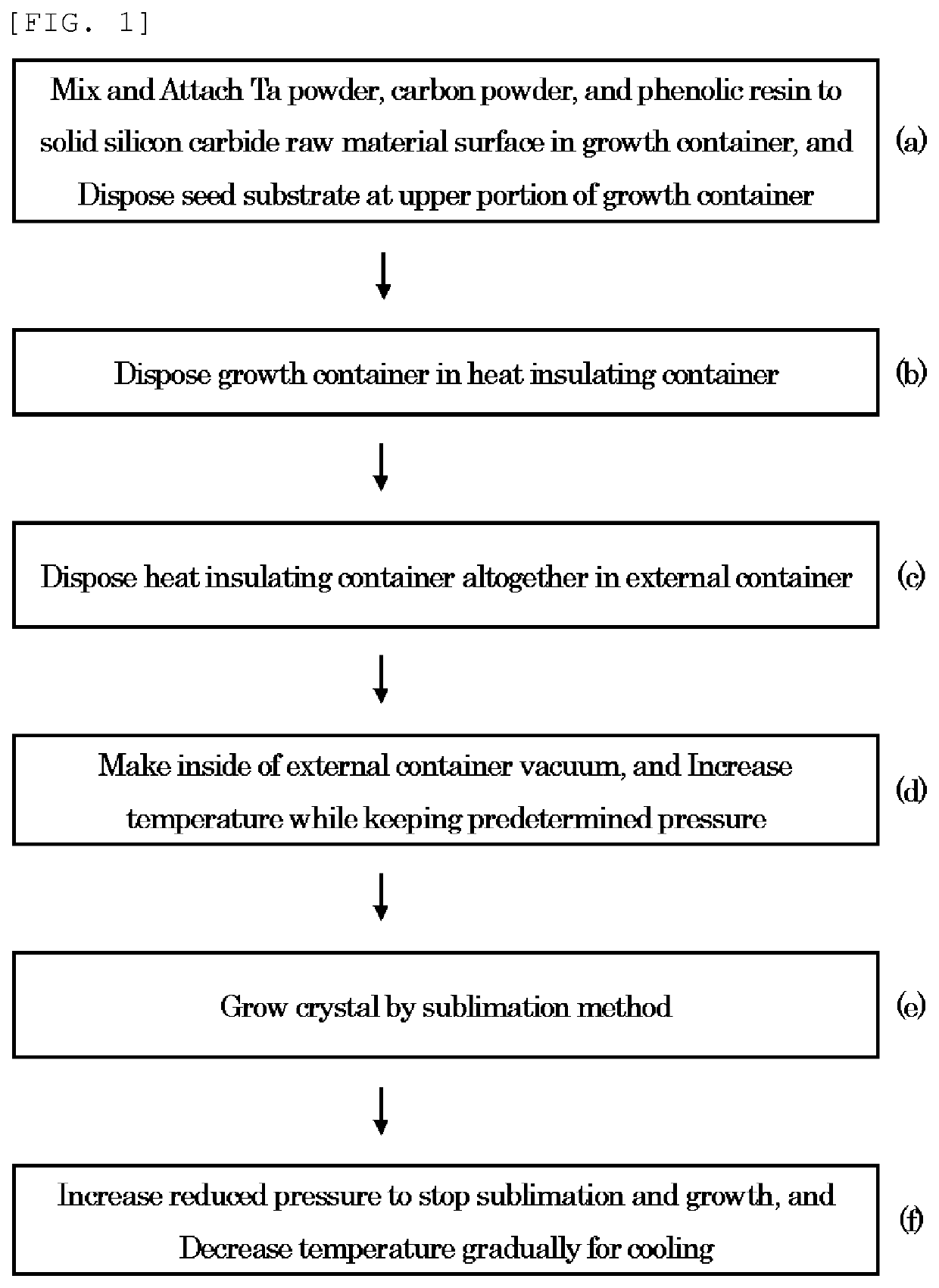
[0037]Herein below, a method for manufacturing a silicon carbide single crystal according to a first embodiment of the present invention will be described with reference to FIGS. 1, 2.
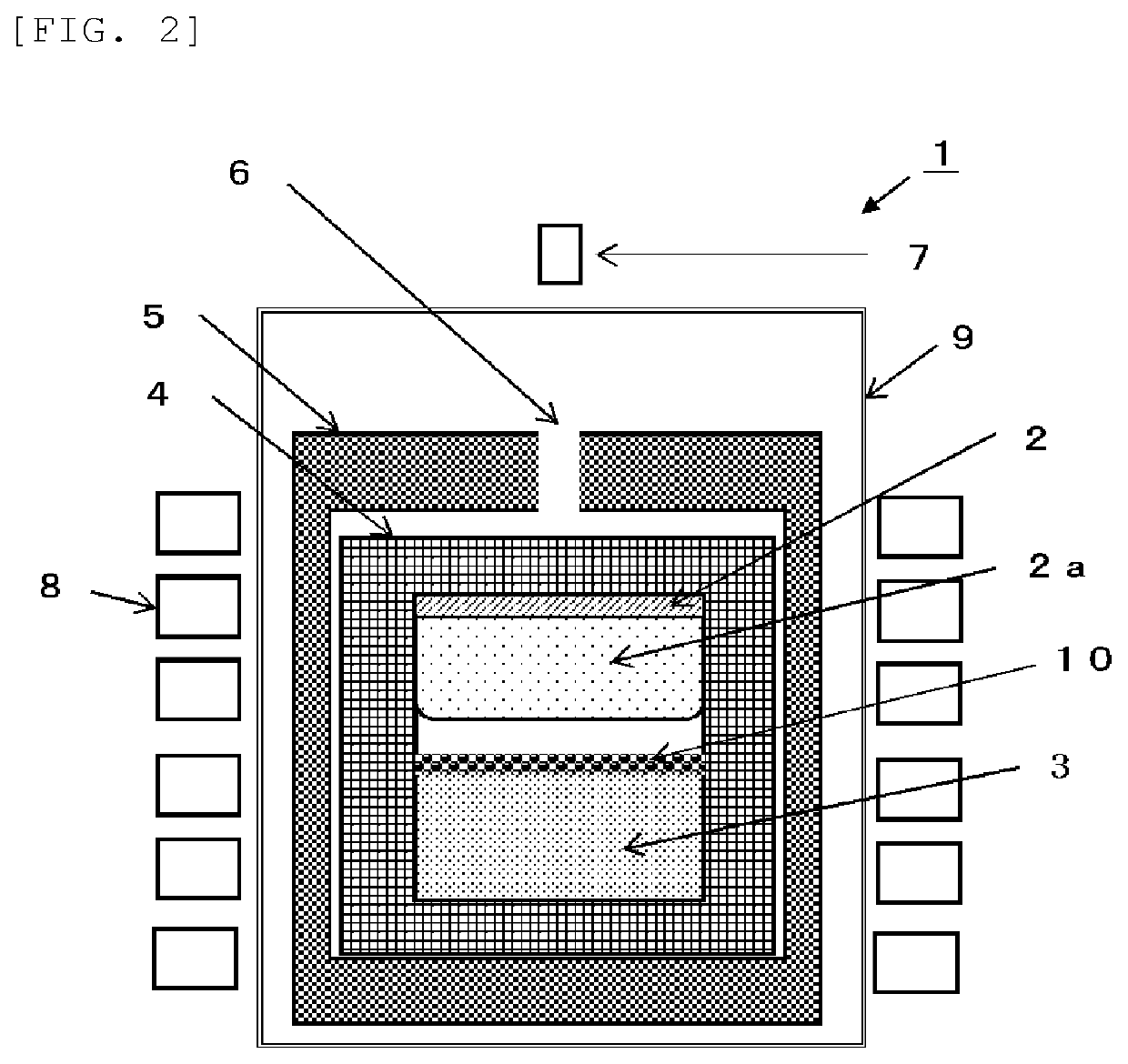
[0038]FIG. 1 is a flowchart showing the method for manufacturing a silicon carbide single crystal according to the first embodiment of the present invention. FIG. 2 is a schematic cross-sectional view of a SiC manufacturing apparatus with which the method for manufacturing a silicon carbide single crystal according to the first embodiment of the present invention can be carried out.
[0039]As shown in FIG. 2, a SiC manufacturing apparatus 1 includes a growth container 4 for housing a seed substrate (seed wafer) 2 and a solid silicon carbide raw material 3, a heat-insulating container 5 surrounding the growth container 4, a temperature-measurement sensor 7 for measuring the temperature inside the growth container 4 via an upper-portion temperature measurement hole 6 provided through the heat-insulating co...
second embodiment
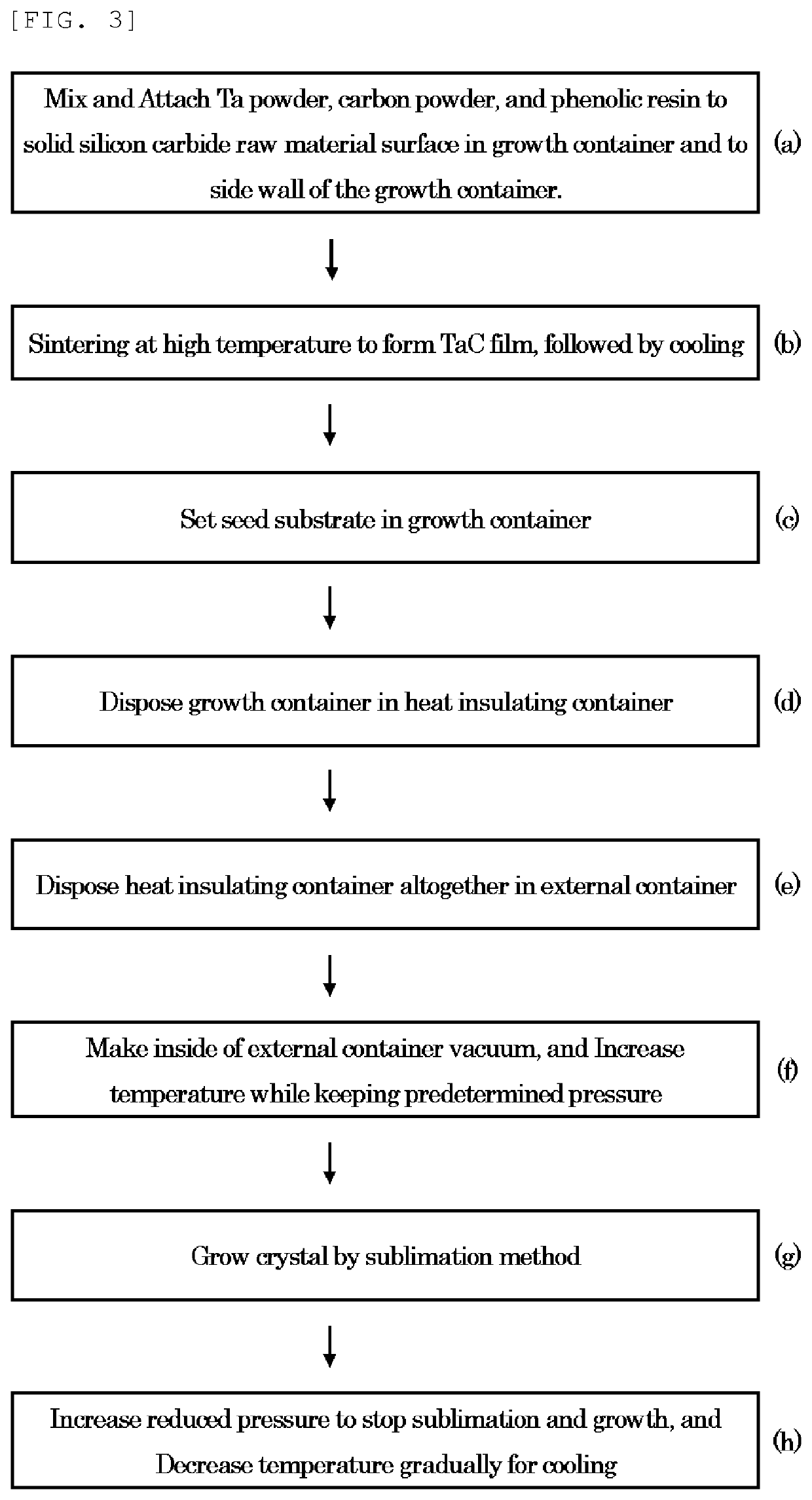
[0048]Next, a method for manufacturing a silicon carbide single crystal according to a second embodiment of the present invention will be described with reference to FIGS. 3, 4.
[0049]FIG. 3 is a flowchart showing the method for manufacturing a silicon carbide single crystal according to the second embodiment of the present invention. FIG. 4 is a schematic cross-sectional view of a SiC manufacturing apparatus with which the method for manufacturing a silicon carbide single crystal according to the second embodiment of the present invention can be carried out. A SiC manufacturing apparatus 1′ in FIG. 4 has the same configuration as that of the SiC manufacturing apparatus 1 in FIG. 2.
[0050]In the method for manufacturing a silicon carbide single crystal according to the second embodiment of the present invention, first, as described in FIG. 3(a), a Ta powder, a carbon powder, and a phenolic resin are mixed together, and attached to the surface of the solid silicon carbide raw material ...
example 1
[0061]Under the following growth conditions, a SiC single crystal with a diameter of 4 inches (100 mm) was grown.
[0062]Seed crystal substrate . . . a SiC single crystal substrate with a diameter of 4 inches (100 mm) and the main surface being tilted by 4° from the {0001} plane in the direction[0063]Growth temperature . . . 2200° C.[0064]Pressure . . . 10 Torr (13 hPa)[0065]Atmosphere . . . argon and nitrogen gases
[0066]The SiC single crystal was prepared according to the procedure as described in FIG. 1 (i.e., the procedure described in the first embodiment).
[0067]The prepared single crystal was sliced. The distribution and average number (density) of carbon inclusions in the wafer plane were examined with a microscope. FIG. 5 shows the result. As can be seen from FIG. 5, the carbon inclusion density in Example 1 was 2.4 / cm2. This shows that significant improvement was achieved in terms of carbon inclusion in comparison with Comparative Example to be described later.
PUM
 Abstract
Description
Claims
Application Information
 - R&D
- Intellectual Property
- Life Sciences
- Materials
- Tech Scout
- Unparalleled Data Quality
- Higher Quality Content
- 60% Fewer Hallucinations
Browse by: Latest US Patents, China's latest patents, Technical Efficacy Thesaurus, Application Domain, Technology Topic, Popular Technical Reports.
© 2025 PatSnap. All rights reserved.Legal|Privacy policy|Modern Slavery Act Transparency Statement|Sitemap|About US| Contact US: help@patsnap.com