Probe card

a technology of probes and insertion holes, which is applied in the field of probe cards, can solve the problems of difficulty in realizing a reduction in size and pitch, high cost of forming through holes, and machining methods using drills or lasers, etc., and achieves the reduction of size and pitch of probe insertion holes, easy handling, and small area

Active Publication Date: 2021-04-08
POINT ENG
View PDF1 Cites 2 Cited by
  • Summary
  • Abstract
  • Description
  • Claims
  • Application Information

AI Technical Summary

Benefits of technology

[0034]In the present invention, by making the guide plate, which serves to guide front ends of the probes, with an anodic oxide film material, it is possible to realize a reduction in size and pitch of the probe insertion holes. In addition, due to the provision of the probe insertion holes, the guide plate substantially defining the probing area may be configured to have a smaller area than the first and second plates supporting the guide plate, thereby making it possible to realize a structure that is easy to handle.
[0035]In addition, by realizing a structure in which the upper and lower guide plates are provided in at least a partial area of the probe head, it is possible to achieve more uniform flatness of the upper and lower guide plates. As a result, it is possible to obtain an effect of improving positional accuracy of the probes in terms of the provision of the probes.
[0036]In addition, by providing the guide plate to have a smaller area than the entire area of the probe head, it is possible to realize a structure in which the surface of a structure supporting the guide plate is exposed, which can be effective in terms of heat dissipation when the structure supporting the guide plate is made of a metal material. Therefore, the probe card can be used more effectively in a burn-in test process.

Problems solved by technology

However, using the machining method in forming the through-hole may result in difficulty in realizing a reduction in size and pitch, which is required in recent semiconductor technologies.
That is, the machining method using the drill or the laser has limitations in realizing a reduction in size and pitch of the through-hole because the through-hole has to be formed in consideration of mechanical errors.
In addition, the machining method using the drill or the laser may require high costs in forming the through-hole.
However, the resin material has poor mechanical strength and the process for forming a through-hole is complicated.
However, etching the silicon material may be problematic in that it is difficult to secure the mechanical strength of the guide plate for the probe card.
Specifically, it is difficult to vertically form the through-hole in the silicon material during the etching process, and thus, the upper and lower inner diameters of the through-hole may be formed differently.
As a result, when forming a plurality of through-holes, the thickness of a partition wall separating adjacent through-holes may become thin, leading to a reduction in the mechanical strength of the guide plate for the probe card, which is problematic.
As such, although the silicon material is easily etched, a disadvantage is that the mechanical strength thereof is poor.
In addition, as the partition wall between the through-holes becomes thin by the etching process of the silicon guide plate for the probe card, the risk of damage may increase when the inner walls of the through-holes are worn due to sliding friction with the probes.
Therefore, there is a problem that it is difficult to secure wear resistance.
Therefore, forming the through-holes in the silicon guide plate for the probe card may require a lot of time and the process may be cumbersome.
In this case, the probe card 100′ is problematic in that it is difficult for heat of the intermediate plate 4 with an elevated temperature to be dissipated due to the structure in which the upper and lower guide plates 2 and 3 cover the intermediate plate 4.
This may result in a change in the positions of the through-holes and a reduction in the positional accuracy of front ends of the probes, thereby causing a problem of measurement error of the probe card 100′.

Method used


Image

  • Probe card
  • Probe card
  • Probe card

Examples


Embodiment Construction

[0046]Contents of the description below merely exemplify the principle of the invention. Therefore, those of ordinary skill in the art may implement the theory of the invention and invent various apparatuses which are included within the concept and the scope of the invention even though it is not clearly explained or illustrated in the description. Furthermore, in principle, all the conditional teams and embodiments listed in this description are clearly intended for the purpose of understanding the concept of the invention, and one should understand that this invention is not limited to the exemplary embodiments and the conditions.

[0047]The above described objectives, features, and advantages will be more apparent through the following detailed description related to the accompanying drawings, and thus those of ordinary skill in the art may easily implement the technical spirit of the invention.

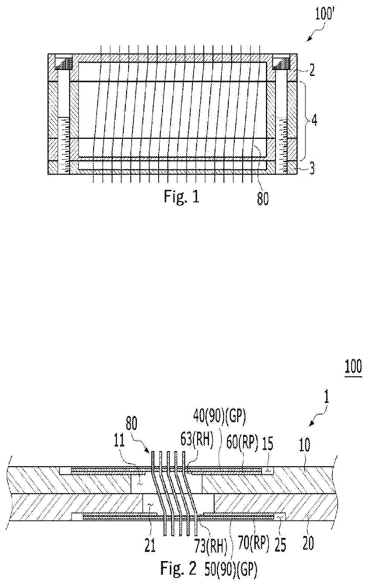
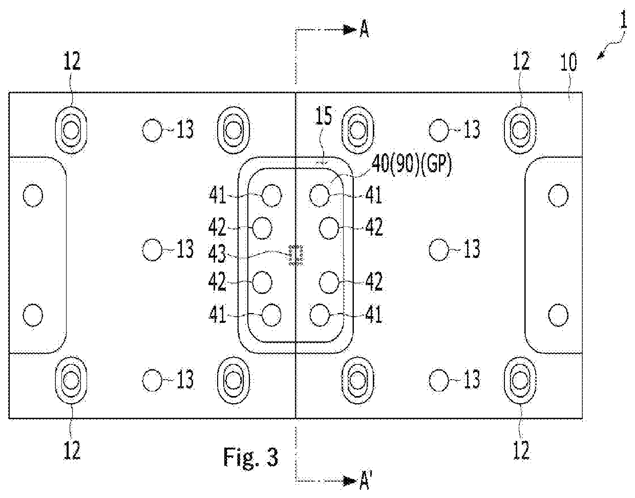
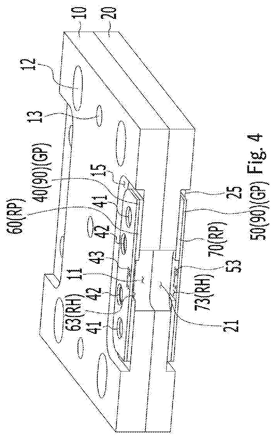
[0048]The embodiments of the present invention will be described with reference to cros...


PUM


Abstract

Proposed is a probe card for performing a circuit test on a wafer and, more particularly, a probe card capable of realizing a reduction in size and pitch of probe insertion holes.

Description

CROSS REFERENCE TO RELATED APPLICATION[0001]The present application claims priority to Korean Patent Application No. 10-2019-0123270, filed Oct. 4, 2019, the entire contents of which is incorporated herein for all purposes by this reference.BACKGROUND OF THE INVENTIONField of the Invention[0002]The present invention relates to a probe card for testing a pattern formed on a wafer.Description of the Related Art[0003]A test for electrical characteristics of semiconductor devices is performed by approaching a semiconductor wafer to a probe card having a plurality of probes on a wiring board, and bringing the respective probes into contact with corresponding electrode pads on the semiconductor wafer. After the probes reach positions where the probes are brought into contact with the electrode pads, the semiconductor wafer may be further lifted by a predetermined height toward the probe card. This process is called overdrive, and the distance over which the wafer is further lifted by a pr...

Claims


Application Information

Patent Timeline
Patent Type & Authority Applications(United States)
IPC IPC(8): G01R1/073G01R31/28
CPCG01R1/07371G01R31/2831G01R1/07342G01R31/2886G01R1/07314G01R1/07357G01R1/07335G01R1/0491
Inventor AHN, BUM MOPARK, SEUNG HOBYUN, SUNG HYUN
Owner POINT ENG
Why Eureka
Try Eureka