

Process for the hetero-integration of a semiconductor material of interest on a silicon substrate
- Summary
- Abstract
- Description
- Claims
- Application Information
AI Technical Summary
Benefits of technology
Problems solved by technology
Method used
Image

Examples
Embodiment Construction
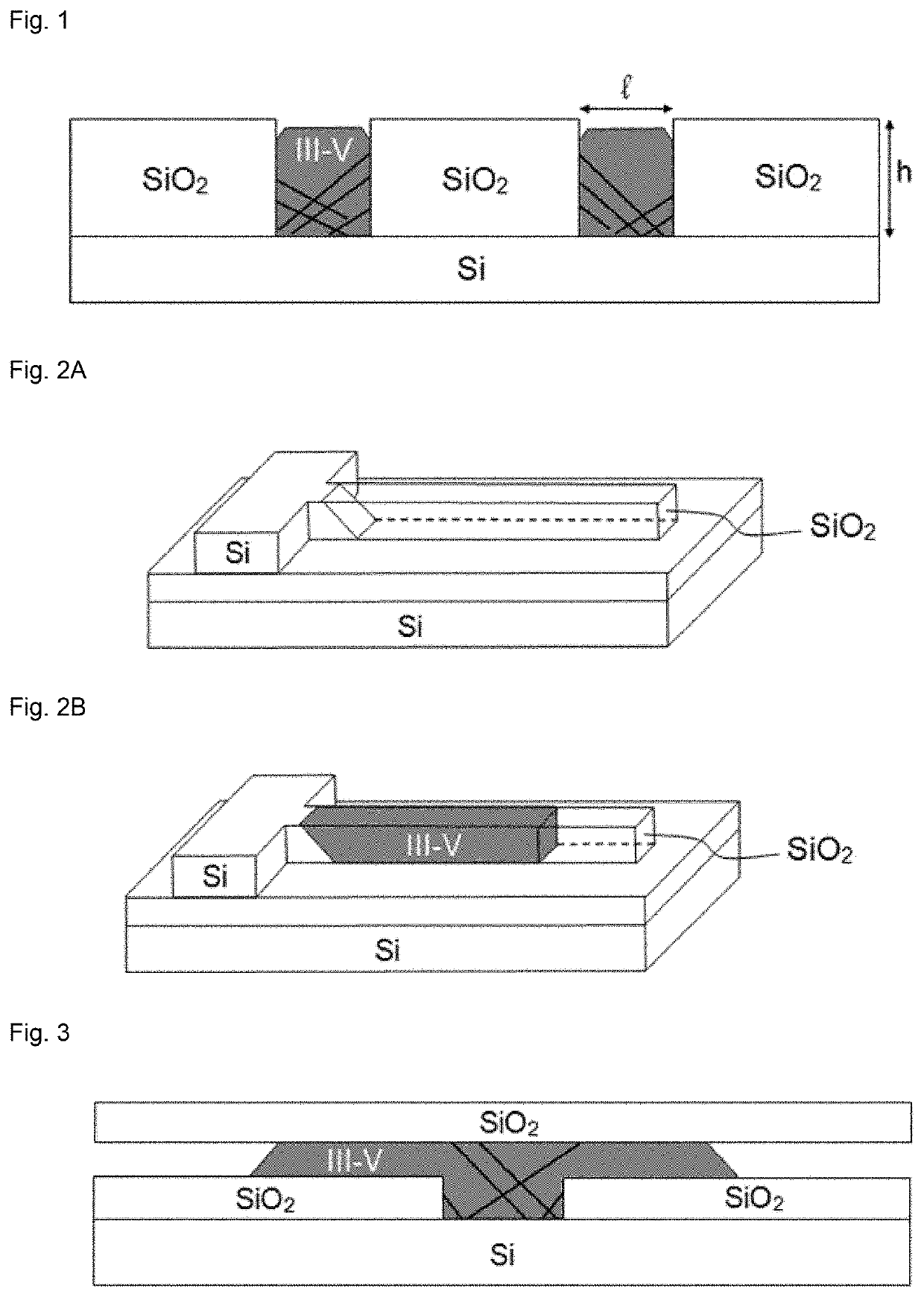
[0085]FIGS. 1, 2A, 2B and 3 (prior art) have been described previously and will not be repeated here.
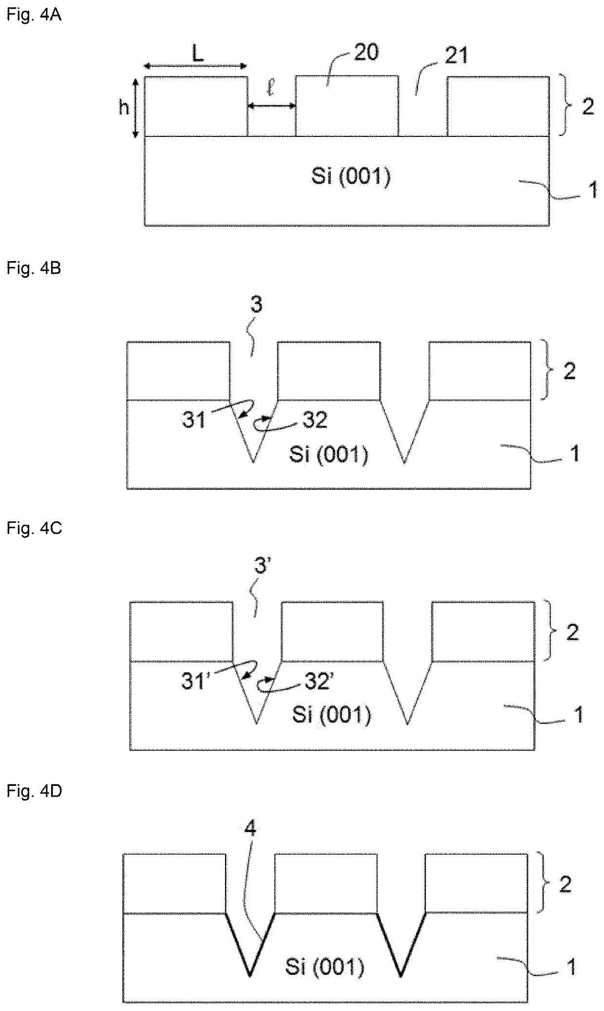
[0086]FIGS. 4A to 4N represent an example and variants of the hetero-integration process according to the invention. In this example, the starting silicon substrate 1 has a [001] crystal orientation and may thus be denoted as Si(001).
[0087]The process comprises a step of structuring the [001] oriented silicon substrate, which comprises a step of making a growth mask 2 on the surface of said substrate (FIG. 4A). The growth mask 2 comprises masking patterns 20. The growth mask is preferably made of a dielectric material, generally SiO2 or SiN, which shows selectivity towards etching relative to the silicon substrate. Two consecutive (or adjacent) masking patterns are separated from each other by a distance 1. This distance 1 corresponds in this example to the width of a trench 21. A trench corresponds to an area of the substrate 1 not masked with the dielectric material (or “exposed ar...
PUM
 Abstract
Description
Claims
Application Information