Manufacturing Method for Array Substrate and Array Substrate

Pending Publication Date: 2021-04-29
CHENGDU ZHONGDIAN PANDA DISPLAY TECH CO LTD
View PDF0 Cites 0 Cited by
  • Summary
  • Abstract
  • Description
  • Claims
  • Application Information

AI Technical Summary

Benefits of technology

[0006]The present disclosure provides a manufacturing method for an array substrate and an array substrate, which only requires fo

Problems solved by technology

The above manufacturing method for an array substrate, including six passes

Method used


Image

  • Manufacturing Method for Array Substrate and Array Substrate
  • Manufacturing Method for Array Substrate and Array Substrate
  • Manufacturing Method for Array Substrate and Array Substrate

Examples


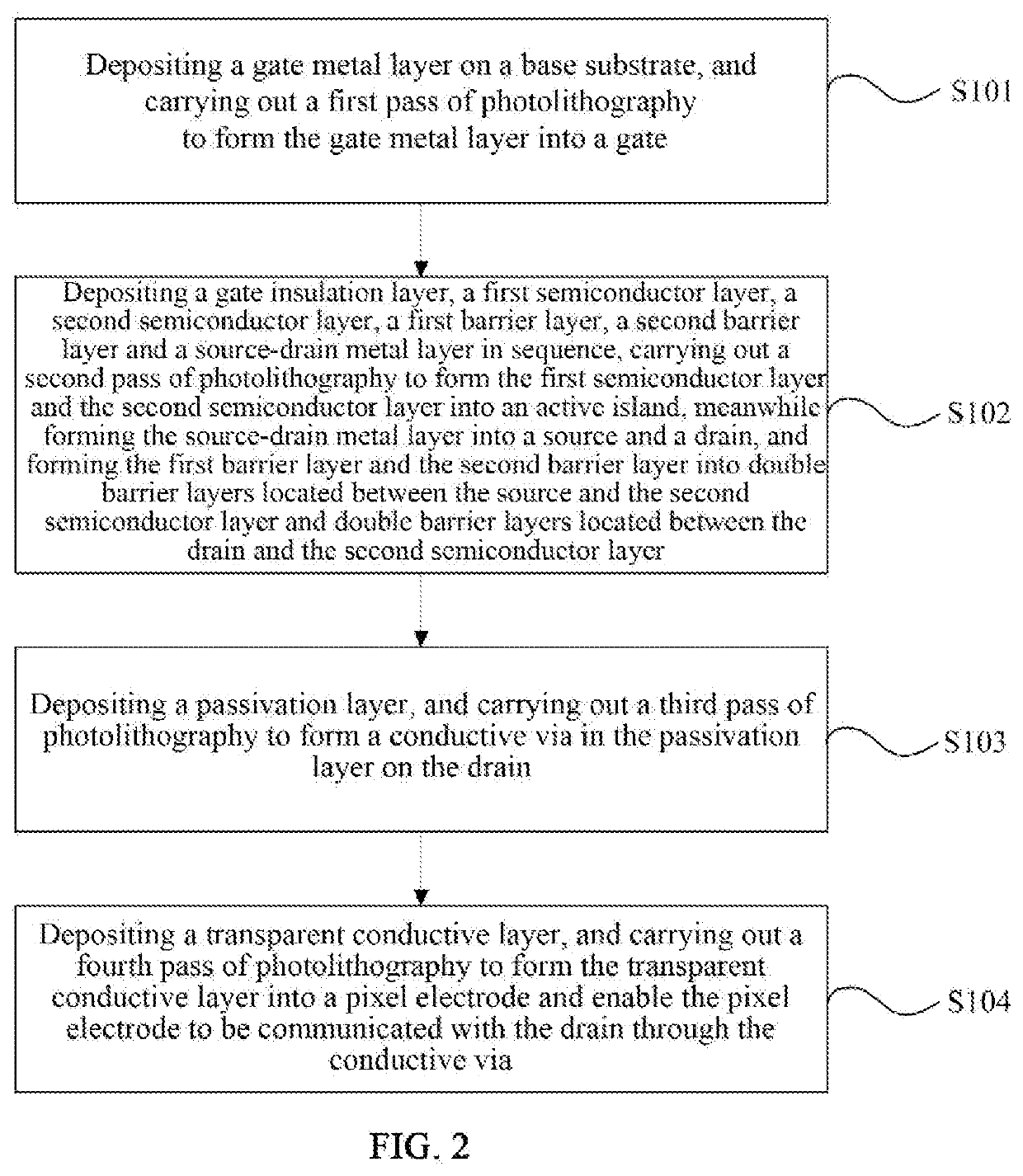
Embodiment Construction

[0063]In order to make objects, technical solutions and advantages of the present disclosure clearer, the technical solutions in the present disclosure will be described clearly and completely below in conjunction with the accompanying drawings in the present disclosure, and apparently, some but not all embodiments of the present disclosure are described. Based on the embodiments of the present disclosure, all other embodiments obtained by those ordinarily skilled in the art without inventive effort shall fall within the scope of protection of the present disclosure.

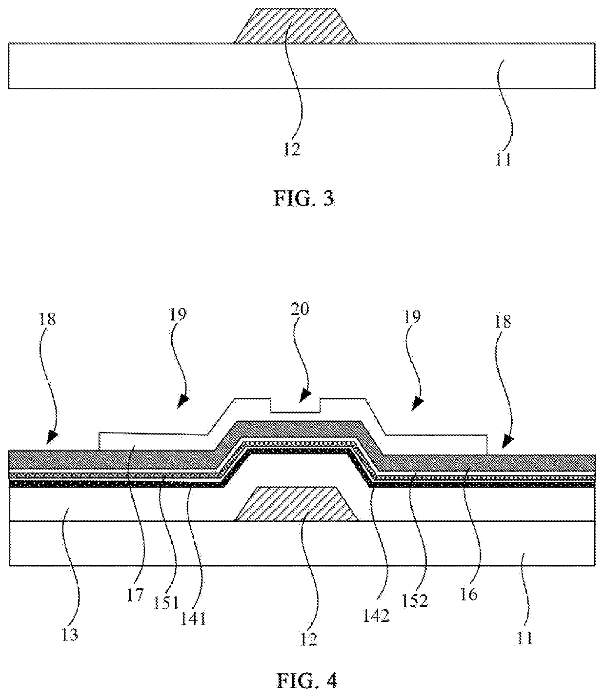
[0064]It should be understood that, a conventional liquid crystal display panel is formed by attaching one thin film transistor array substrate (“TFT Array Substrate” for short) and one color filter substrate (“CF Substrate” for short), a pixel electrode and a common electrode are formed on the array substrate and the color filter substrate, respectively, and liquid crystal is injected between the array substrate and the...


PUM


Abstract

Provided is a manufacturing method for an array substrate and an array substrate. The manufacturing method for an array substrate comprises: depositing a gate metal layer, and carrying out a first pass of photolithography to form a gate; depositing a gate insulation layer, a first semiconductor layer, a second semiconductor layer, a first barrier layer, a second barrier layer and a source-drain metal layer in sequence, carrying out a second pass of photolithography to form an active island, meanwhile forming a source and a drain; depositing a passivation layer, and carrying out a third pass of photolithography to form a conductive via in the passivation layer on the drain; and depositing a transparent conductive layer, and carrying out a fourth pass of photolithography to form the transparent conductive layer into the pixel electrode and enable the pixel electrode to be communicated with the drain through the conductive via.

Description

CROSS-REFERENCE TO RELATED APPLICATION[0001]The present disclosure claims the priority to the Chinese patent application with the filing number CN201911013106.4, filed on Oct. 23, 2019 with the China Patent Office, and entitled “Manufacturing Method for Array Substrate and Array Substrate”, which is incorporated herein by reference in entirety.TECHNICAL FIELD[0002]The present disclosure relates to the technical field of liquid crystal display, in particular to a manufacturing method for an array substrate and an array substrate.BACKGROUND ART[0003]With the development of display technology, flat panel display devices such as liquid crystal display (“LCD” for short), due to advantages such as high image quality, power saving, thin body and no radiation, are widely applied in various consumer electronic products such as mobile phones, televisions, personal digital assistants and notebook computers, and become mainstream in display devices. A liquid crystal display panel is generally c...

Claims


Application Information

Patent Timeline
IPC IPC(8): H01L27/12H01L29/786H01L29/66
CPCH01L27/1288H01L27/1225G02F1/1368H01L29/66969H01L29/78693G02F1/136236G02F1/136231
Inventor LIU, XIANGSUN, XUEJUNLI, GUANGSHENGMA, QUN
Owner CHENGDU ZHONGDIAN PANDA DISPLAY TECH CO LTD
Why Eureka
Try Eureka