
Method and system for jfet with implant isolation

a technology of implant isolation and isolation method, which is applied in the direction of diodes, semiconductor devices, electrical apparatus, etc., can solve problems such as undesirable, and achieve the effects of reducing the parasitic inductance and resistance of the interconnect, reducing the complexity of the board, and reducing the cost of the packag

Active Publication Date: 2021-06-24
NEXGEN POWER SYST INC
View PDF2 Cites 1 Cited by
  • Summary
  • Abstract
  • Description
  • Claims
  • Application Information

AI Technical Summary

Benefits of technology

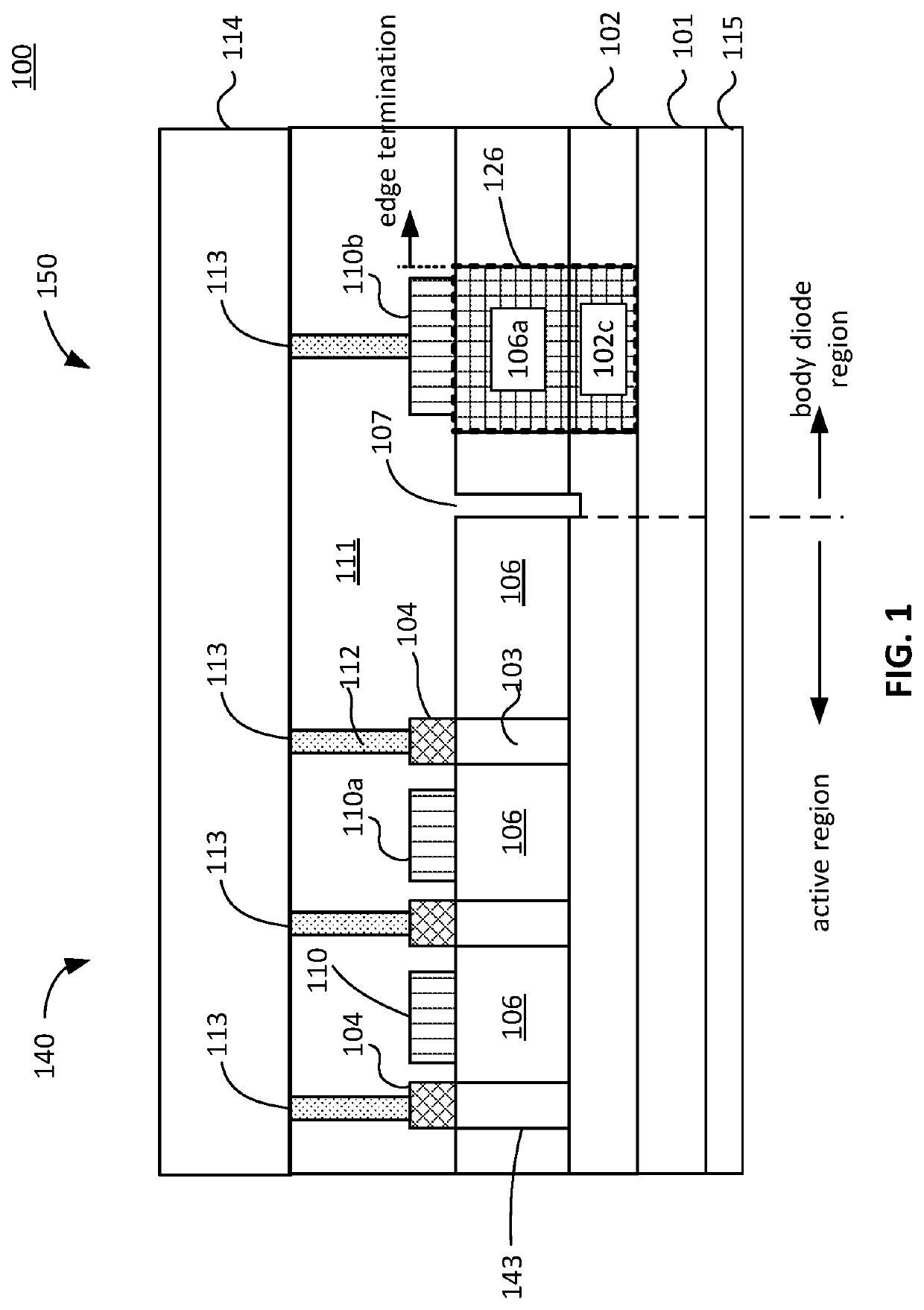
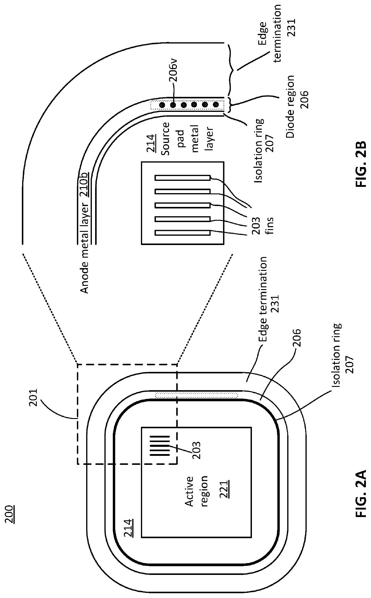
The present invention provides vertical JFET devices with a monolithically integrated source to drain connected body diode. This integration reduces interconnects between the transistor and the diode terminals, which reduces part count, complexity, and board space, resulting in a more cost-effective and compact device. The integrated diode can be used for various circuit applications, such as preventing high voltage build-up and improving switching speed and efficiency. The use of GaN as the diode material provides fast switching and low power loss. The MPS diode structure achieves low turn-on voltage and low reverse bias leakage.

Problems solved by technology

A gate driver circuit would need to be able to handle this current, which is not desirable.

Method used


Image

  • Method and system for jfet with implant isolation
  • Method and system for jfet with implant isolation
  • Method and system for jfet with implant isolation

Examples


Embodiment Construction

[0021]It should be understood that the drawings are not drawn to scale, and similar reference numbers are used for representing similar elements. As used herein, the terms “example embodiment,”“exemplary embodiment,” and “present embodiment” do not necessarily refer to a single embodiment, although it may, and various example embodiments may be readily combined and interchanged, without departing from the scope or spirit of the present invention. Furthermore, the terminology as used herein is for the purpose of describing example embodiments only and is not intended to be a limitation of the invention. In this respect, as used herein, the term “in” may include “in” and “on”, and the terms “a”, “an” and “the” may include singular and plural references. Furthermore, as used herein, the term “by” may also mean “from”, depending on the context. Furthermore, as used herein, the term “if” may also mean “when” or “upon”, depending on the context. Furthermore, as used herein, the words “and...


PUM


Abstract

A vertical junction field effect transistor (JFET) includes a substrate, an active region having a plurality of semiconductor fins, a source metal layer on an upper surface of the fins, a source metal pad layer coupled to the semiconductor fins through the source metal layer, a gate region surrounding the semiconductor fins, and a body diode surrounding the gate region

Description

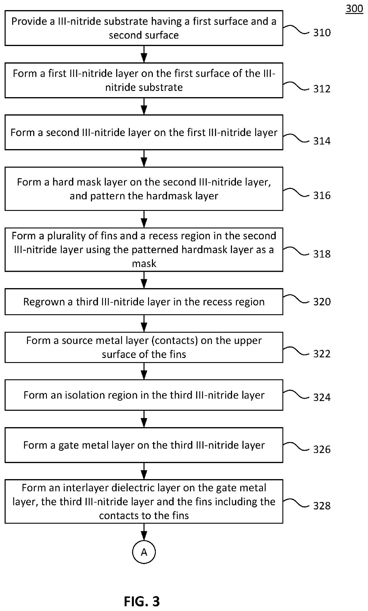
CROSS-REFERENCES TO RELATED APPLICATIONS[0001]This application claims priority to U.S. Provisional Patent Application No. 62 / 953,059, filed on Dec. 23, 2019, entitled “Method and System for JFET with Implant Isolation,” the disclosure of which is hereby incorporated by reference in its entirety for all purposes.BACKGROUND OF THE INVENTION[0002]Power electronics are widely used in a variety of applications. For example, power electronic devices are commonly used in power switching applications. Typical devices that are currently used for power applications are metal-oxide-semiconductor field effect transistors (MOSFET) and insulated gate bipolar transistors (IGBT).SUMMARY OF THE INVENTION[0003]Embodiments of the present invention provide novel vertical JFET devices with a monolithically integrated source to drain connected body diode. Monolithic integration, rather than using a co-packaged diode, can reduce the parasitic inductance and resistance of the interconnects between the tran...

Claims


Application Information

Patent Timeline
IPC IPC(8): H01L29/808H01L29/66H01L27/06H01L27/088H01L29/78H01L29/06H01L29/20
CPCH01L29/8083H01L29/66909H01L27/0676H01L29/2003H01L29/785H01L29/0642H01L27/0886H01L29/7302H01L27/0629H01L29/732H01L29/6631H01L21/8252H01L29/861H01L29/872H01L29/0619H01L29/66924H01L29/66212H01L27/0727H01L27/0605
Inventor DROWLEY, CLIFFORDEDWARDS, ANDREW P.PIDAPARTHI, SUBHASH SRINIVASMILANO, RAY
Owner NEXGEN POWER SYST INC
Learn More