
Film touch sensor and structure including the same

a technology of touch sensor and film, which is applied in the direction of conductive materials, insulating supports, synthetic resin layered products, etc., can solve the problems of difficult to remove the sacrificial layer, metal wirings and the base film and the metal wirings of the wiring substrate cannot be completely peeled off from the substrate, etc., to achieve excellent peelability, increase process efficiency and productivity, and improve the effect of manufacturing the touch sensor

Active Publication Date: 2021-09-09
DONGWOO FINE CHEM CO LTD
View PDF0 Cites 0 Cited by
  • Summary
  • Abstract
  • Description
  • Claims
  • Application Information

AI Technical Summary

Benefits of technology

The present invention allows for improved efficiency and productivity in manufacturing touch sensors by using an insulation layer and an adhesive layer on a transparent conductive film pattern. Additionally, a separation layer is formed on a carrier substrate for use as a protective covering during separation. The touch sensor is then formed on the substrate for increased accuracy and heat resistance. The process of removing the separation layer is simplified by not requiring it. The thin film formed using the specific curable composition described in the invention has excellent peelability, withstanding heating and solvents, and can be used as a resin base film for manufacturing a circuit through photolithography. The thin film has excellent crack-suppressing properties and peel-off strength, making it advantageous for use in touch sensor structures.

Problems solved by technology

However, in a case of using the inorganic peeling-off agent in the above method, when peeling-off the base film and the metal wirings from the substrate, the metal wirings and the base film are not smoothly peeled-off therefrom, such that a portion of the metal wirings or the base film is remained on the surface of the substrate, and an organic material used as the peeling-off agent comes out on the metal wirings and the surface of the base film.
That is, there is a problem that, even if using the peeling-off agent, the metal wirings of a wiring substrate cannot be completely peeled-off from the substrate.
However, the above-described method has problems that, in a case of having a large size, it is difficult to remove the sacrificial layer in the removing process thereof, and various types of base film may not be used because performing a high-temperature process is impossible.

Method used


Image

  • Film touch sensor and structure including the same
  • Film touch sensor and structure including the same
  • Film touch sensor and structure including the same

Examples


examples and synthesis examples

PREPARATIVE EXAMPLES AND SYNTHESIS EXAMPLES

[0213]1. Preparation of Polymers as a Component of Curable Resin Composition

[0214]As a component of the curable resin composition, polymers were prepared as follows.

[Preparative Example 1] Preparation of Polymer A-1

[0215]4-benzoyloxy-3-hydroxycyclohexylmethyl methacrylate represented by Formula 1-1 below was used as a monomer, and 100 parts by weight (‘wt. parts’) thereof was dissolved in propylene glycol monomethyl ether (PGME) so as to be an amount of 30 wt. parts. The obtained solution was heated to 80° C. while blowing a nitrogen gas thereinto, 2,2′-azobisisobutyronitrile (AIBN) was added thereto in an amount of 5 mol % to a total weight of the monomer, and then a reaction was carried out at 80° C. for 8 hours to prepare Polymer A-1. A weight average molecular weight (MW) of the prepared polymer was measured by gel filtration chromatography, and the measured result was 25,000.

[Preparative Example 2] Preparation of Polymer A-2

[0216]Polym...

synthesis example 1

[0232]1.6 wt. parts of Polymer A-1, 3.2 wt. parts of hexamethoxymethyl melamine represented by Formula B-1 below as a cross-linking agent, and 0.2 wt. parts of pyridinium-p-toluenesulfonic acid as a polymerization catalyst were dissolved in 95 wt. parts of propylene glycol monomethyl ether (PGME) to obtain a solution. The obtained solution was applied to soda glass having a thickness of 0.7 mm and alkali-free glass having a thickness of 0.5 mm, respectively, by spin coating, and then heat-treated at 150° C. or higher for 30 minutes to form a film having a thickness of about 300 nm.

synthesis example 2

[0233]2.4 wt. parts of Polymer A-1, 2.4 wt. parts of hexamethoxymethyl melamine (Formula B-1) as a cross-linking agent and 0.2 wt. parts of pyridinium-p-toluenesulfonic acid as a polymerization catalyst were dissolved in 95 wt. parts of propylene glycol monomethyl ether (PGME) to obtain a solution. The obtained solution was applied to soda glass and alkali-free glass, respectively, and then heat-treated similar to Synthesis Example 1 to form a film having a thickness of about 300 nm.


PUM

PropertyMeasurementUnit
thicknessaaaaaaaaaa
heat resistanceaaaaaaaaaa

Abstract

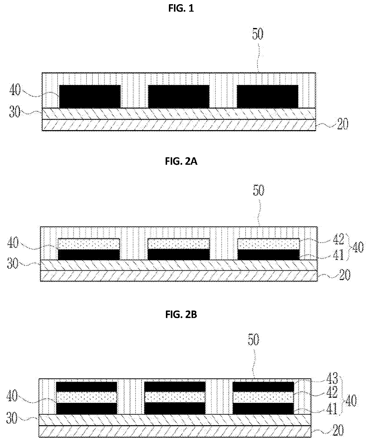
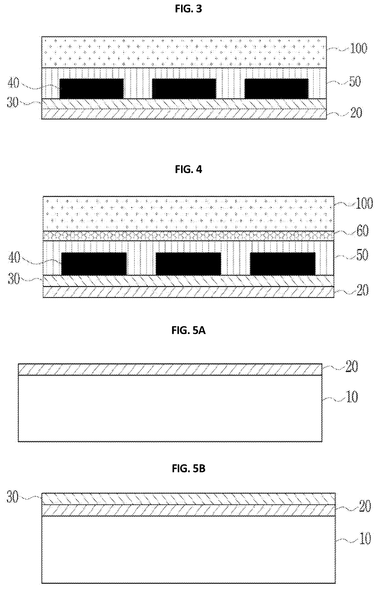
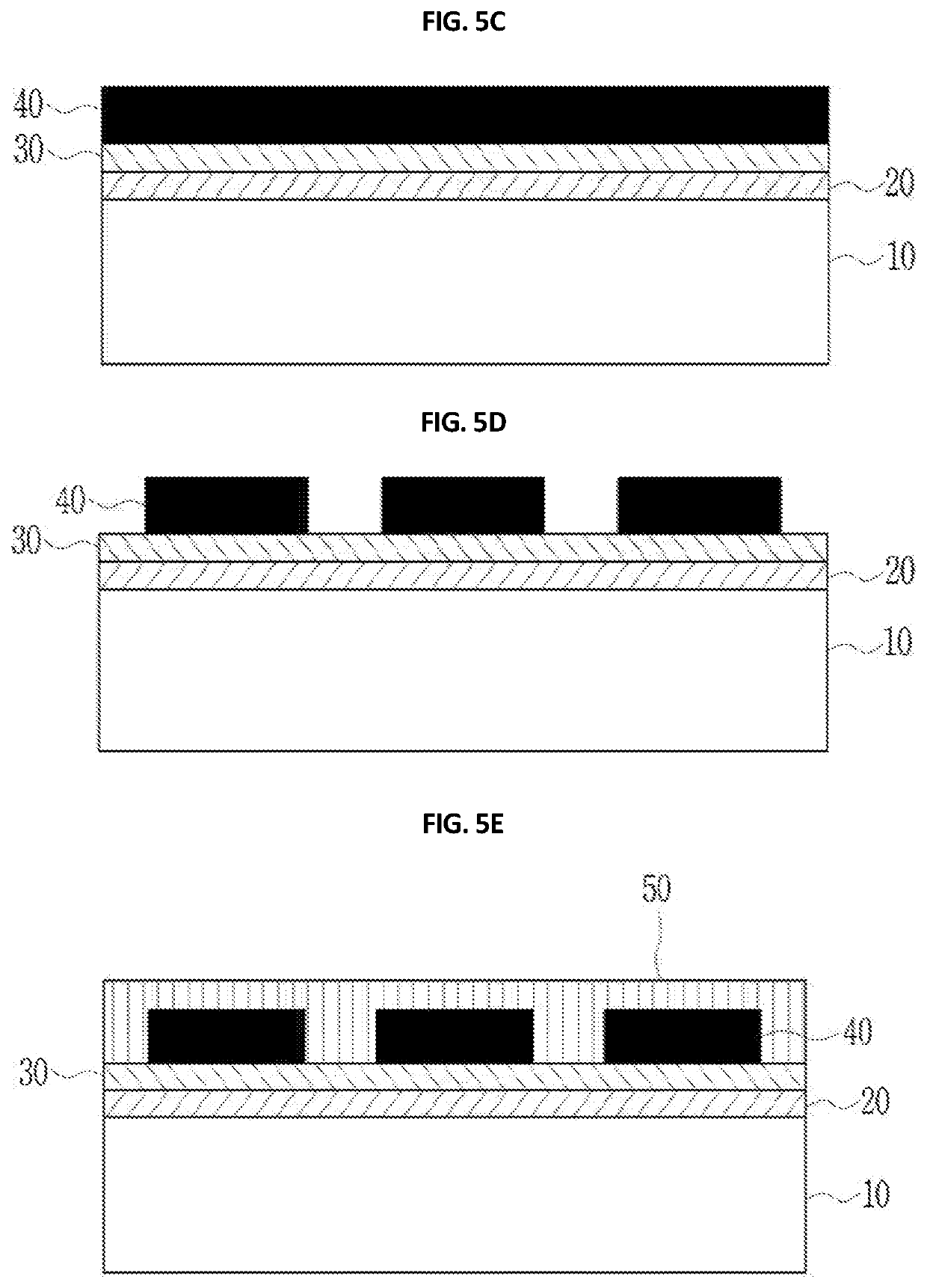
A film touch sensor is prepared by performing a process in which a separation layer made of a specific component is formed on a carrier substrate, and an insulation film is formed on a transparent conductive film pattern, which is used as a planarization layer, an adhesive layer or a base layer.

Description

BACKGROUND OF THE INVENTION1. Field of the Invention[0001]The present invention relates to a film touch sensor and a structure including the film touch sensor.2. Description of the Related Art[0002]Attempts are being made to introduce a touch input type into a wider variety of electronic devices due to the touch input type being in the spotlight as a next-generation input type. Accordingly, research and development for a touch sensor capable of being applied to different environments and accurately recognizing a touch have been actively executed.[0003]For example, in a case of the electronic device having a touch input type display, an ultrathin flexible display which achieves an ultralight and a low power consumption with improved portability is in the spotlight as a next-generation display, and thus the development for a touch sensor applicable to such a display is required.[0004]The flexible display refers to a display fabricated on a flexible substrate which is capable of being ...

Claims


Application Information

Patent Timeline
Patent Type & Authority Applications(United States)
IPC IPC(8): C08F20/20H01B5/14C08F12/08C08F20/40G06F3/041
CPCC08F20/20H01B5/14G06F2203/04102C08F20/40G06F3/041C08F12/08G03F7/004H01B1/02H01B1/04H01B1/12C08F212/08B32B7/12B32B2255/10B32B27/16B32B27/308B32B27/306B32B2255/28B32B27/18B32B2457/208B32B27/34B32B2255/26B32B2307/732B32B5/18B32B27/286B32B27/302B32B27/285B32B23/08B32B27/38B32B27/32B32B2270/00B32B27/281B32B27/22B32B27/40B32B23/20B32B2307/412B32B27/365B32B2255/20B32B2307/42B32B27/36B32B27/065B32B27/288B32B27/304B32B27/20B32B27/08G06F2203/04103G06F2203/04112G06F3/044G02B5/3033C08F120/30C08F120/20C08F220/303C08F220/20C08F220/1804C08F220/14G03F7/0048H01B1/124G02B1/18G06F3/0443B32B7/10C08F20/14
Inventor YU, BYUNG MUKPARK, MIN HYUKAN, MYUNG YOUNG
Owner DONGWOO FINE CHEM CO LTD
Learn More