Silicon carbide seed crystal and method of manufacturing the same, and method of manufacturing silicon carbide ingot

a technology of silicon carbide and seed crystal, which is applied in the direction of carbide, polycrystalline material growth, crystal growth process, etc., can solve the problems of increasing the manufacturing cost of crystal growth and affecting the yield, and achieve the effect of fewer defects

Active Publication Date: 2022-01-27
GLOBALWAFERS CO LTD
View PDF1 Cites 0 Cited by
  • Summary
  • Abstract
  • Description
  • Claims
  • Application Information

AI Technical Summary

Benefits of technology

[0006]The disclosure provides a silicon carbide seed crystal, and the basal plane dislocations (BPD) density difference of the two opposite surfaces is low, which allows a more consistent crystal growth direction and can reduce the structural defects of the silicon carbide ingots grown from the silicon carbide seed crystal. Moreover, the silicon carbide seed crystal can be reused, so the cost of silicon carbide growth is saved.
[0007]The disclosure also provides a method of manufacturing a silicon carbide crystal, which is used to form the silicon carbide seed crystal. Accordingly, after being processed, the formed seed crystals can be used as silicon carbide seed crystals in another silicon carbide ingot manufacturing process, so that the processed silicon carbide seed crystal can be reused, and the cost of crystal growth can be reduced.
[0008]The disclosure further provides a method of manufacturing silicon carbide ingots, which uses the silicon carbide seed crystals to grow high-quality silicon carbide ingots with fewer defects.
[0015]Based on the above, the silicon carbide seed crystal of the disclosure allows a consistent seed crystal growth direction by controlling the basal plane dislocation density difference between the silicon surface and the carbon surface to produce high-quality silicon carbide ingots with fewer defects. The disclosure provides a method of manufacturing a silicon carbide seed crystal, and accordingly a silicon carbide seed crystal with a small basal plane dislocation density difference between the silicon surface and the carbon surface can be formed, and the seed crystal can be reused in the crystal growth process.

Problems solved by technology

For example, taking the silicon carbide crystal as an example, if the quality of the silicon carbide crystal is not good, many defects may accordingly occur due to different growth directions during the crystal growth process, and the yield is affected.
However, in the prior art, after a silicon carbide seed crystal is used to grow silicon carbide ingots, the silicon carbide seed crystal cannot be reused because there are greater stress and more defects in and around the silicon carbide crystal, resulting in the increase of the manufacturing cost of crystal growth.

Method used


Image

  • Silicon carbide seed crystal and method of manufacturing the same, and method of manufacturing silicon carbide ingot
  • Silicon carbide seed crystal and method of manufacturing the same, and method of manufacturing silicon carbide ingot
  • Silicon carbide seed crystal and method of manufacturing the same, and method of manufacturing silicon carbide ingot

Examples


preparation example 1-9

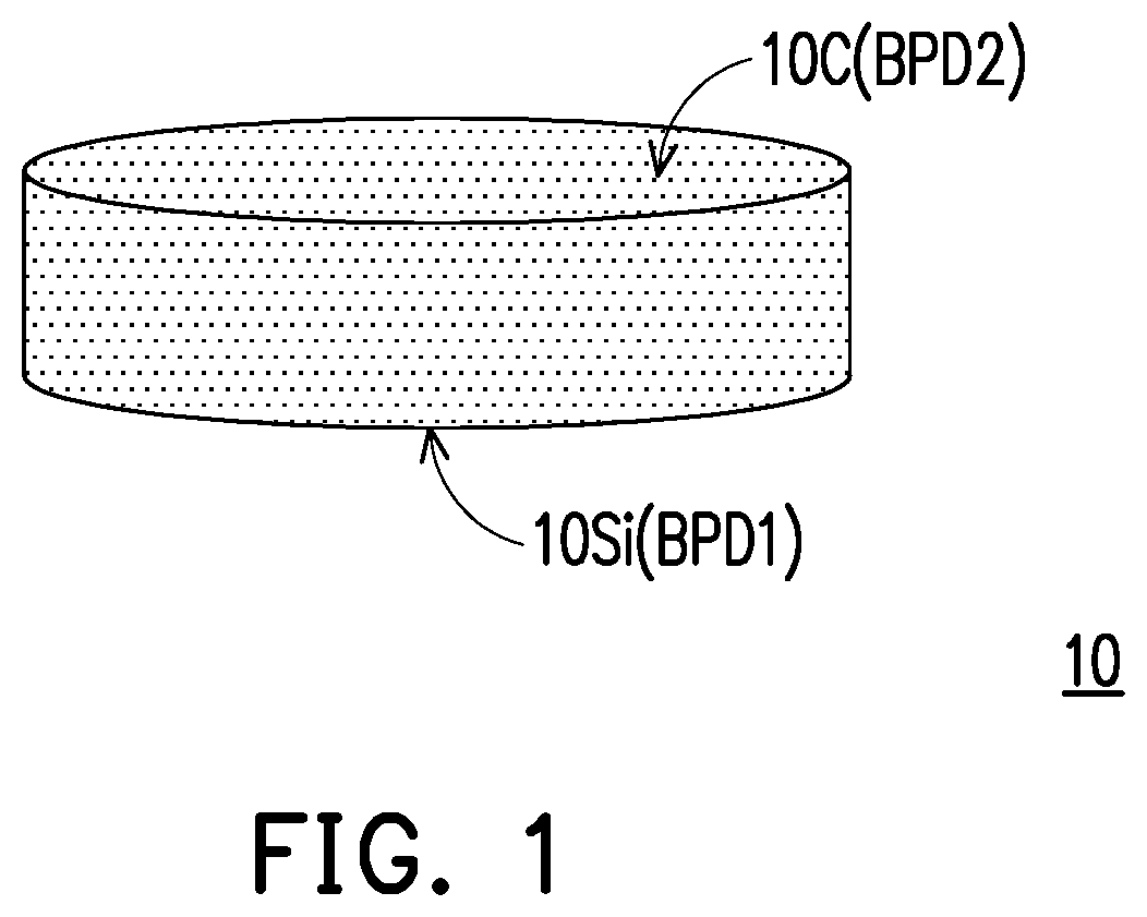
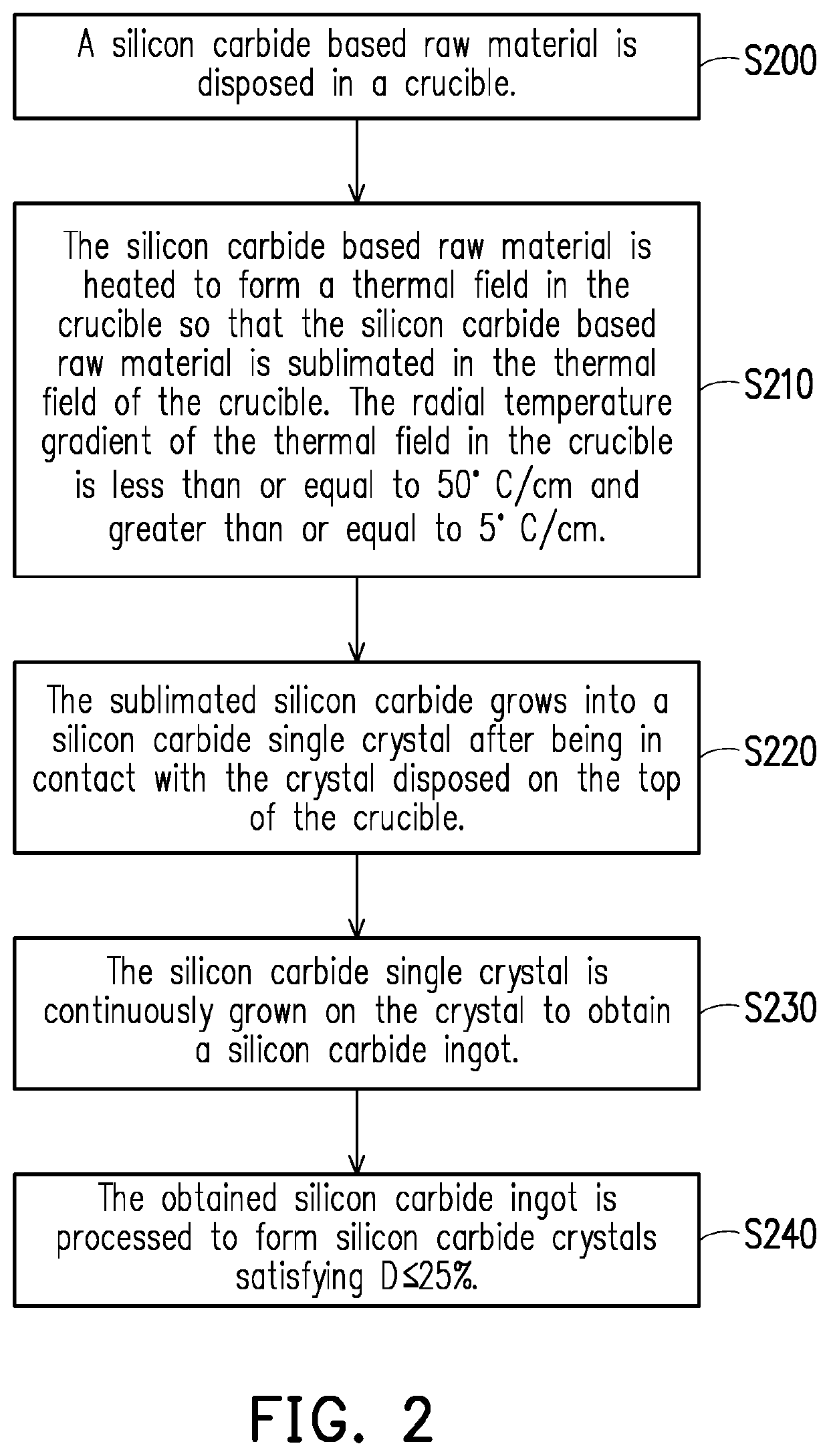
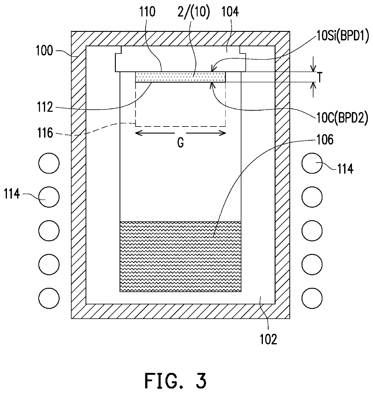
[0053]In the device shown in FIG. 3, a silicon carbide based raw material is disposed in a crucible, and the silicon carbide based raw material is heated. The temperature gradient is adjusted to form thermal fields with different radial temperature gradients in the crucible. As shown in Table 1 below, the temperature gradient of Comparative Examples 1-3 is greater than 50° C. / cm, and the temperature gradient of Examples 1-6 is less than or equal to 50° C. / cm. In Example 1 of Table 1 below, a thermal field with a radial temperature gradient of 15° C. / cm is formed in the crucible. Next, the silicon carbide based raw material is sublimated in the thermal field of the crucible. Then, the sublimated silicon carbide is in contact with the original seed crystal 2 (or the reusable silicon carbide seed crystal 10) disposed on the top of the crucible to grow a silicon carbide single crystal on the seed crystal. The silicon carbide single crystal is continuously grown on the original seed crys...


PUM

PropertyMeasurementUnit
dislocation densityaaaaaaaaaa
radial temperatureaaaaaaaaaa
stacking faultaaaaaaaaaa

Abstract

A silicon carbide seed crystal and method of manufacturing the same, and method of manufacturing silicon carbide ingot are provided. The silicon carbide seed crystal has a silicon surface and a carbon surface opposite to the silicon surface. A difference D between a basal plane dislocation density BPD1 of the silicon surface BPD1 and a basal plane dislocation density BPD2 of the carbon surface satisfies the following formula (1):D=(BPD1−BPD2) / BPD1≤25%  (1).

Description

CROSS-REFERENCE TO RELATED APPLICATION[0001]This application claims the priority benefit of U.S. provisional application Ser. No. 63 / 056,728, filed on Jul. 27, 2020 and U.S. provisional application Ser. No. 63 / 056,729, filed on Jul. 27, 2020. The entirety of each of the above-mentioned patent applications is hereby incorporated by reference herein and made a part of this specification.BACKGROUNDTechnology Field[0002]The disclosure relates to a semiconductor seed crystal and a method of manufacturing the same, and a method of manufacturing a semiconductor ingot, and particularly relates to a silicon carbide seed crystal and a manufacturing method thereof.Description of Related Art[0003]In the semiconductor industry, the method of manufacturing wafers includes first forming an ingot, and then slicing the ingot to obtain a wafer. The ingot is manufactured in a high-temperature environment, for example. In a common ingot manufacturing method, a seed crystal is disposed in a high-tempera...

Claims


Application Information

Patent Timeline
Patent Type & Authority Applications(United States)
IPC IPC(8): C30B23/06C30B23/02C30B29/36
CPCC30B23/066C30B29/36C30B23/025C30B23/002C30B23/063C01B32/956H01L29/30
Inventor LIN, CHING-SHAN
Owner GLOBALWAFERS CO LTD
Why Eureka
Try Eureka