
Eureka
For R&D, Eureka makes reading and utilizing patents & technical documents easy.
Eureka AIR
Designed for self-driven R&D workflows. Generate viable solutions, solve complex R&D challenges, empower your innovation with AI.

Eureka Materials
Designed for material experts only. Revolutionize your material R&D, from search, analyze, to developing new materials.

TechResearch
Generate reliable direction feasibility study reports for your R&D in just a few steps.

TechSeek
Discover and master advanced knowledge NOW. Basics, ideas, possibilities, all at once.

TechMind
As an expert in R&D Theories, TechMind can generates customized viable solutions instantly.

TechRisk
Analyze your overall solution with one click, know your potential R&D risks in advance.

TechMonitor
Get weekly tech updates, stay abreast of the latest tech innovations and key insights.
Light emitting element and display device using same
- Summary
- Abstract
- Description
- Claims
- Application Information
AI Technical Summary
Benefits of technology
Problems solved by technology
Method used
Image

Examples
first embodiment
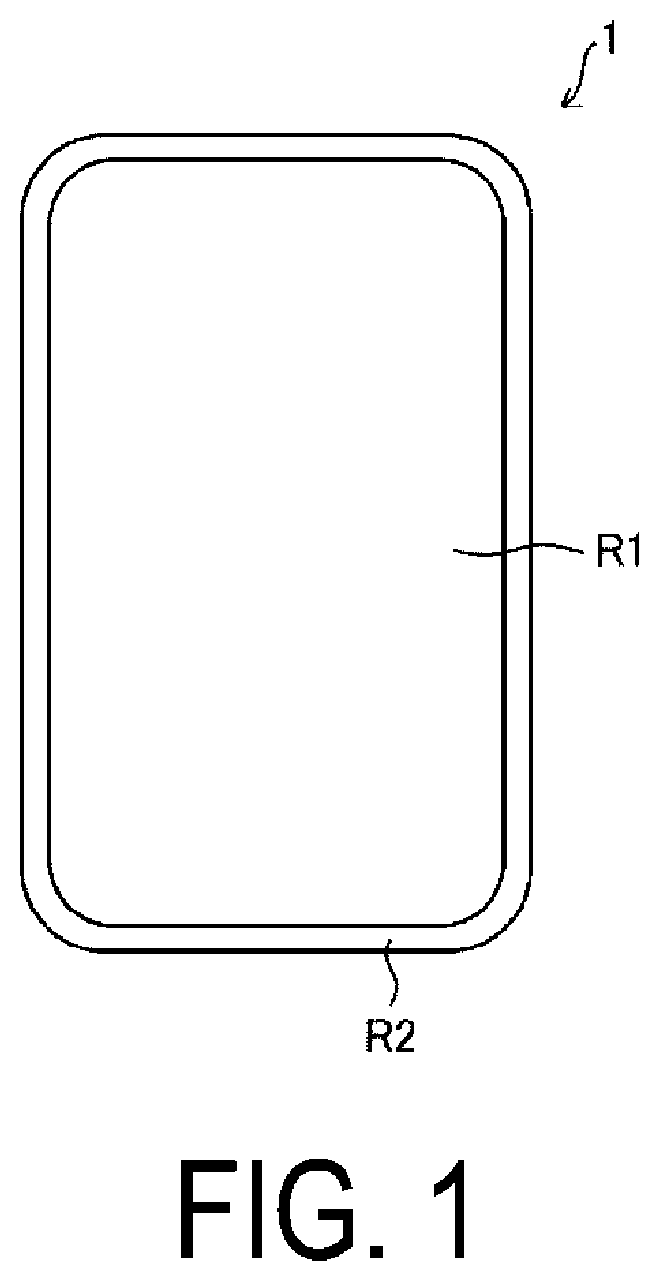
[0017]FIG. 1 is a diagram of a display device 1 according to the first embodiment. The display device 1 uses a small panel of a mobile device such as a smart phone and includes a display region R1 in which a plurality of display pixels D are formed in a matrix-like arrangement and a frame region R2 disposed around the display region R1.
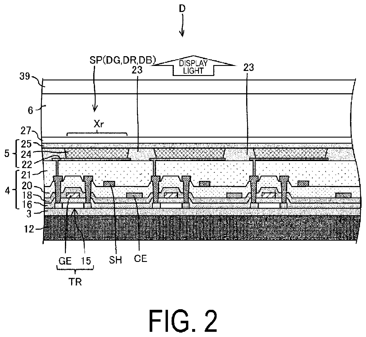
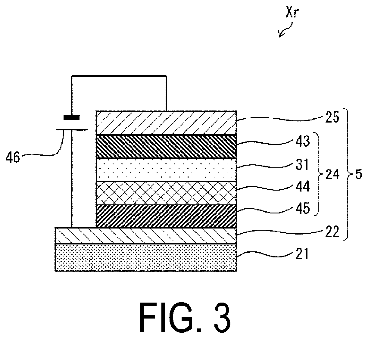
[0018]FIG. 2 is a cross-sectional view of the display pixel D provided in the display region R1 of the display device 1. FIG. 3 is a cross-sectional view of a light-emitting element Xi provided in the display pixel D.
[0019]A substrate 12 may be a glass substrate or a flexible substrate including a resin film such as polyimide. A flexible substrate can also be formed by sandwiching an inorganic insulating film with two resin films. A film made of PET or the like may be applied to the lower surface of the substrate 12. By using a flexible substrate as the substrate 12, a (flexible) display device 1 with flexibility can be formed.
[0020]The barrier layer ...
second embodiment
[0045]FIG. 5(a) is a cross-sectional view focused on a light-emitting layer 31A formed in a light-emitting element Xr1 according to the second embodiment. Constituent elements similar to the constituent elements described above are given the same reference numerals, and detailed descriptions thereof are not repeated.
[0046]In the light-emitting layer 31A, a quantum dot layer 42 is formed by a portion of a plurality of core-shell quantum dot phosphors 41 (a first quantum dot layer), and another quantum dot layer 42 is formed by another portion of the plurality of core-shell quantum dot phosphors 41 (second quantum dot layer). A p-type dopant layer 49 formed by the p-type dopant 51 is disposed between the quantum dot layer 42 and the other quantum dot. layer 42. The p-type dopant layer 49 includes ZnS, and the p-type dopant 51 of the p-type dopant layer 49 includes Cu or Ag.
[0047]FIG. 5(b) is a cross-sectional view illustrating a modified example of the light-emitting layer 31A, and FI...
third embodiment
[0059]FIG. 6(a) is a cross-sectional view focused on a light-emitting layer 31B according to the third embodiment, and FIG. 6(b) is a cross-sectional view illustrating the configuration of a quantum dot phosphor 41A provided in the light-emitting layer 31B. Constituent elements similar to the constituent elements described above are given the same reference numerals, and detailed descriptions thereof are not repeated.
[0060]The quantum dot phosphor 41A includes the core 47, the shell 48 formed around the core 47, and a modifying group 50 that protects the quantum dot phosphor 41A. The modifying group 50 includes an end portion 52 formed from a p-type organic semiconductor disposed on the opposite side of the modifying group 50 from the core 47 and a base portion 53 formed from a material other than a p-type organic semiconductor disposed on the core 47 side of the modifying group 50.
[0061]A quantum dot layer 42 is formed by a portion of a plurality of the quantum dot phosphors 41A, a...
PUM
 Abstract
Description
Claims
Application Information
 - R&D Engineer
- R&D Manager
- IP Professional
- Industry Leading Data Capabilities
- Powerful AI technology
- Patent DNA Extraction
Browse by: Latest US Patents, China's latest patents, Technical Efficacy Thesaurus, Application Domain, Technology Topic, Popular Technical Reports.
© 2024 PatSnap. All rights reserved.Legal|Privacy policy|Modern Slavery Act Transparency Statement|Sitemap|About US| Contact US: help@patsnap.com