Optical semiconductor device

Pending Publication Date: 2022-05-26
LUMENTUM JAPAN INC
View PDF2 Cites 0 Cited by
  • Summary
  • Abstract
  • Description
  • Claims
  • Application Information

AI Technical Summary

Benefits of technology

[0008]In some implementations, the optical semicondu

Problems solved by technology

Further, some manufacturing processes suppress abnormal growth of the burial layer.
When Au diffusion progresses and reaches an active layer (e.g., a multiple-quantum well layer), characteristics and reliability of the optical semiconductor device degrade.
Pt can suppress diffusion of Au into

Method used


Image

  • Optical semiconductor device
  • Optical semiconductor device
  • Optical semiconductor device

Examples


Example

[0023]Some implementations are specifically described in detail in the following with reference to the attached drawings. Note that, throughout the figures for illustrating the implementations, like reference numerals are used to represent members having like functions, and description thereof is omitted for the sake of simplicity. Note that, the drawings referred to in the following are only for illustrating the implementations by way of examples, and are not necessarily drawn to scale.

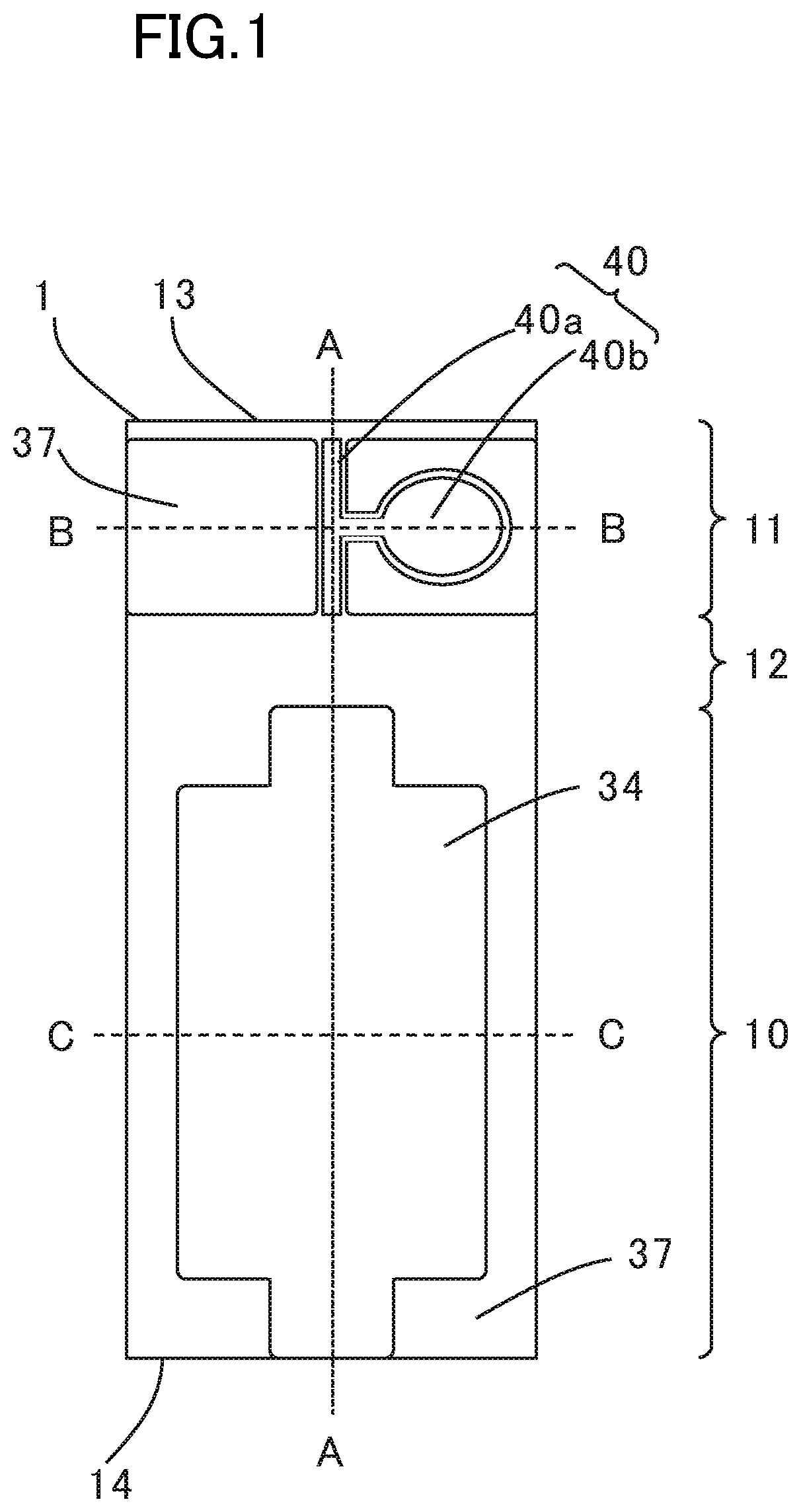
[0024]FIG. 1 is a top view of an example optical semiconductor device 1. The optical semiconductor device 1 may be a modulator-integrated semiconductor laser in which a semiconductor laser 10 and an electro-absorption modulator (EA modulator) 11 are integrated. While an integrated example is described herein, implementations include just the semiconductor laser or just the EA modulator. The optical semiconductor device 1 may be an integrated device in which the semiconductor laser 10, a waveguide 12,...


PUM


Abstract

To provide an optical semiconductor device having excellent long-term reliability, the optical semiconductor device includes: a substrate; a mesa structure provided on the substrate; a semiconductor burial layer provided in contact with two sides of the mesa structure; and an electrode containing Au, which is provided above the semiconductor burial layer. The mesa structure includes a first conductivity type semiconductor layer, a multiple-quantum well layer, and a second conductivity type semiconductor layer, which are stacked in the stated order from a substrate side. The semiconductor burial layer includes a first semi-insulating InP layer provided in contact with side portions of the mesa structure, a first anti-diffusion layer provided in contact with the first semi-insulating InP layer, and a second semi-insulating InP layer provided on the first anti-diffusion layer. The first anti-diffusion layer has an Au diffusion constant that is smaller than that of the first semi-insulating InP layer.

Description

CROSS REFERENCE TO RELATED APPLICATION[0001]The present application claims priority from Japanese patent application JP 2021-017749 filed on Feb. 5, 2021, which claims priority from Japanese Application No. JP 2020-194960 filed on Nov. 25, 2020, the contents of which are hereby expressly incorporated by reference herein.TECHNICAL FIELD[0002]The present invention relates to an optical semiconductor device.BACKGROUND[0003]Recently, with the spread of mobile terminals, and the Internet and other communication devices, optical transceivers are required provide increased speed and capacity. In many cases, optical semiconductor devices are used as light sources of the optical transceivers. An optical semiconductor device can include a buried hetero-structure (BH structure), in which both side surfaces of a mesa structure that includes a multiple quantum well layer are buried in a semiconductor layer. Such a semiconductor device typically has high reliability, high high-speed responsivity,...

Claims


Application Information

Patent Timeline
IPC IPC(8): H01S5/22H01S5/026H01S5/227H01S5/12
CPCH01S5/2218H01S5/0265H01S5/34H01S5/227H01S5/12H01S5/2206H01S5/2275H01S5/34306H01S2301/173H01S5/04252H01S2301/176H01S5/2224H01S5/3235
Inventor NAKAMURA, ATSUSHITAKITA, HAYATOHAMADA, SHIGETAKANAKAJIMA, RYOSUKEARASAWA, MASATOSHIWASHINO, RYU
Owner LUMENTUM JAPAN INC
Why Eureka
Try Eureka