

Sinterable bonding material and semiconductor device using the same
- Summary
- Abstract
- Description
- Claims
- Application Information
AI Technical Summary
Benefits of technology
Problems solved by technology
Method used
Image

Examples
example 1
Preparation of Bonding Material
[0178]A silver filler, resin particles, an additive agent, and a solvent were mixed at a proportion shown in Table 1 to prepare a bonding material.
Evaluation of Warpage
[0179]The obtained bonding material was printed at a thickness of 100 μm on a substrate (a silver-plated copper lead frame, 25×25 mm, a thickness of 0.3 mm). A semiconductor chip (backside silver-plated Si die, 10×10 mm) was mounted on the substrate. The substrate with the chip was dried at 90° C. for 30 minutes, and heated under conditions of 300° C. / 5 minutes / 10 MPa in an oven to obtain a test piece for evaluation. The thickness of the bonded layer after sintering was about 40 to 60 μm.
[0180]Warpage generated by sintering process was measured by using a three-dimensional length measuring machine (KS-1100 manufactured by Keyence Corporation).
Evaluation of Thermal Conductivity
[0181]The obtained bonding material was printed at a thickness of 100 μm between two substrates (silver-plated co...
reference example 1
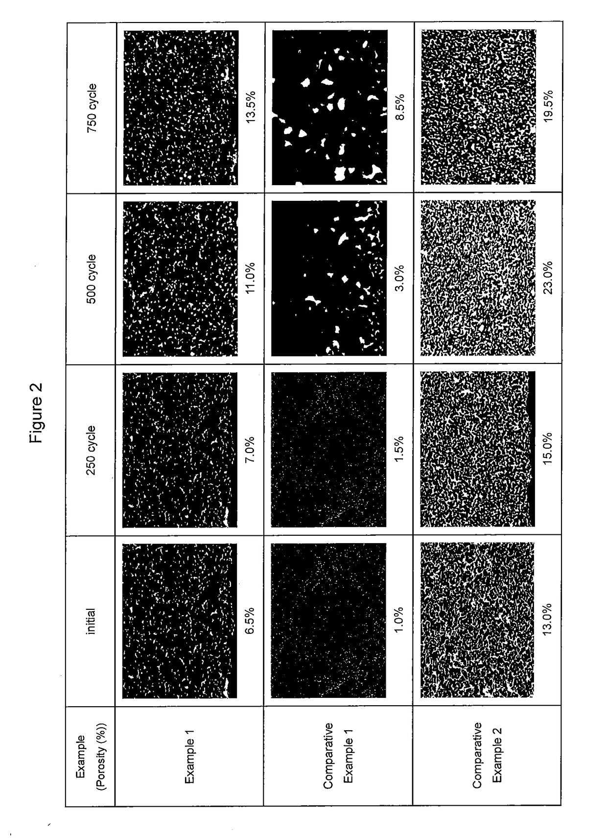
[0198]A silver filler, resin particles, an additive and a solvent at a proportion shown in Table 1, and a liquid epoxy resin (bisphenol A type epoxy resin containing imidazole) in an amount of 1.0% by mass of the total mass of the bonding material were mixed to prepare a bonding material. The obtained bonding material was evaluated in the same manner as in Example 1. The results are shown in Table 1, and FIG. 3.
TABLE 1Example ComparativeComparativeReference1Example 1Example 2Example 1Bonding Materialsilver fillerfiller 1filler 1filler 2filler 1(89.9 wt %)(94.9 wt %)(90.24 wt %)(89.9 wt %)resinresin 1——resin 1(5.0 wt %) (5.0 wt %) additiveDBUDBUPerbutyl DDBU(0.2 wt %) (0.2 wt %) (0.2 wt %) (0.2 wt %) solventBCBCBCA / DPGBC(4.9 wt %) (4.9 wt %) 1 / 1(4.9 wt %) (9.56 wt %) Thermal 175270200 115Conductivity(W / mK)Stress Reduction Test (Measurement of warpage (μm))Chip139170160149Substrate330470410375Reliability Test(Measurement of porosity before and after cooling-heating cycle (%))initial6....
PUM
| Property | Measurement | Unit |
|---|---|---|
| Temperature | aaaaa | aaaaa |
| Pressure | aaaaa | aaaaa |
| Percent by mass | aaaaa | aaaaa |
Abstract
Description
Claims
Application Information