
See-through thin film solar cell module and method of manufacturing the same

Pending Publication Date: 2022-06-02
KOREA INST OF SCI & TECH
View PDF0 Cites 0 Cited by
  • Summary
  • Abstract
  • Description
  • Claims
  • Application Information

AI Technical Summary

Benefits of technology

The present invention provides a see-through thin film solar cell module with high transparency and high-efficiency photovoltaic performance. The module includes a transparent substrate, a first back electrode, a second back electrode, an absorber layer, a laser scribing pattern, and a transparent electrode layer. The second back electrode is made of a molybdenum (Mo) layer with a thickness less than 2 nm and a see-through array pattern. The method of manufacturing the module includes depositing layers, performing laser scribing processes, and depositing additional layers. The technical effects of the invention include improved transparency, high-efficiency photovoltaic performance, and the absence of residue and damage to the back electrode.

Problems solved by technology

However, the highest photovoltaic efficiency of those solar cells is low, e.g., about 10% to about 15%, and thus a technological level of the transparent solar cells does not reach an efficiency of 8% (at an average visible light transmittance of 30%).
In addition, the dye-sensitized solar cells or the organic solar cells lack constituent material stability and thus are not suitable for solar cell power plants which require long-term use.
However, because the existing see-through chalcogenide thin film solar cell technology uses mechanical scribing, a see-through region has a very large line width noticeable by the naked eye and an aperture pattern is not precise, thereby greatly reducing aesthetic properties of products.
As such, heat energy of the incident laser beam L may not be easily concentrated on the interfacial region H2 and thus a pattern formed by the laser beam may greatly differ from a designed pattern in shape or size to cause excessively irregular processing (see reference symbol I in FIG. 19).
In this case, shunting between cells may occur, or irregularity may be caused in subsequent thin film deposition, and visibility may deteriorate in the case of the pattern P4.

Method used


Image

  • See-through thin film solar cell module and method of manufacturing the same
  • See-through thin film solar cell module and method of manufacturing the same
  • See-through thin film solar cell module and method of manufacturing the same

Examples


Embodiment Construction

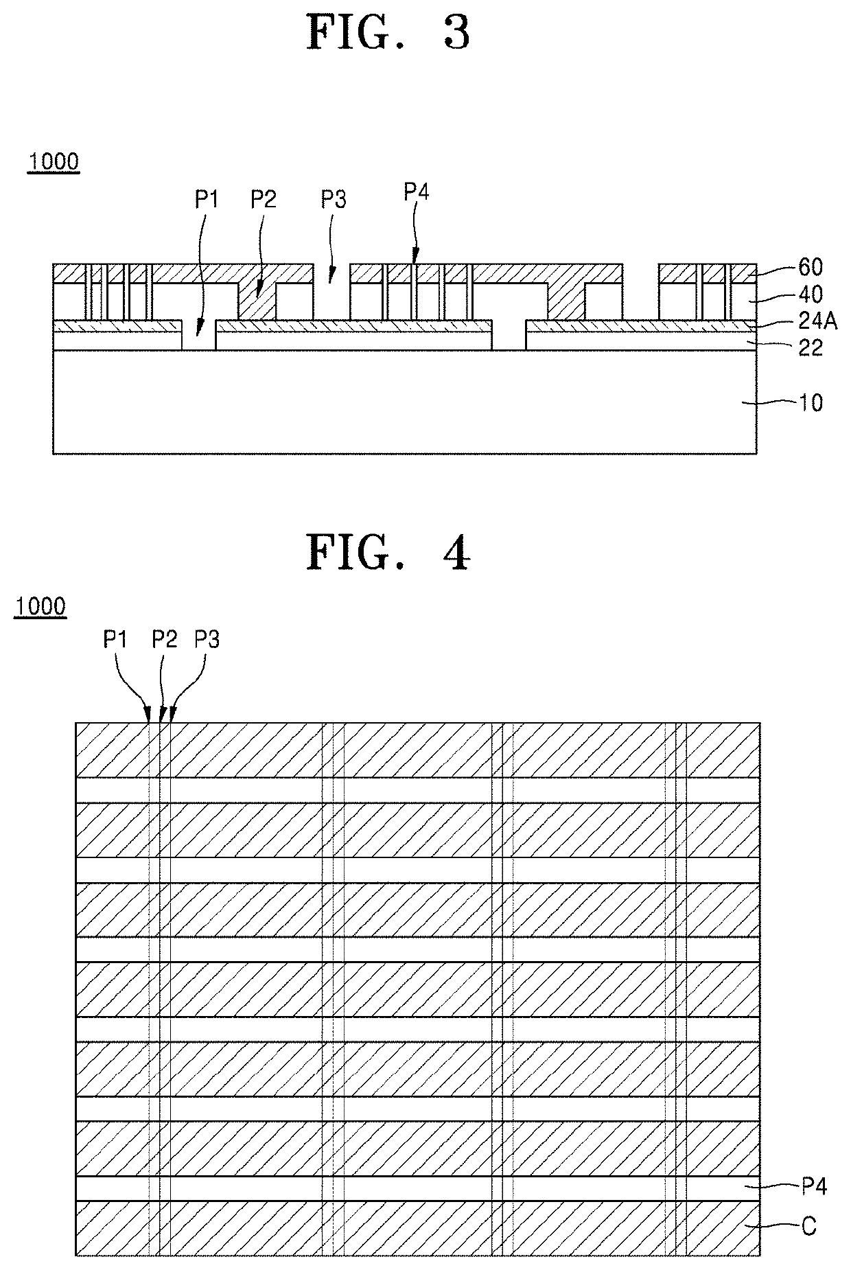
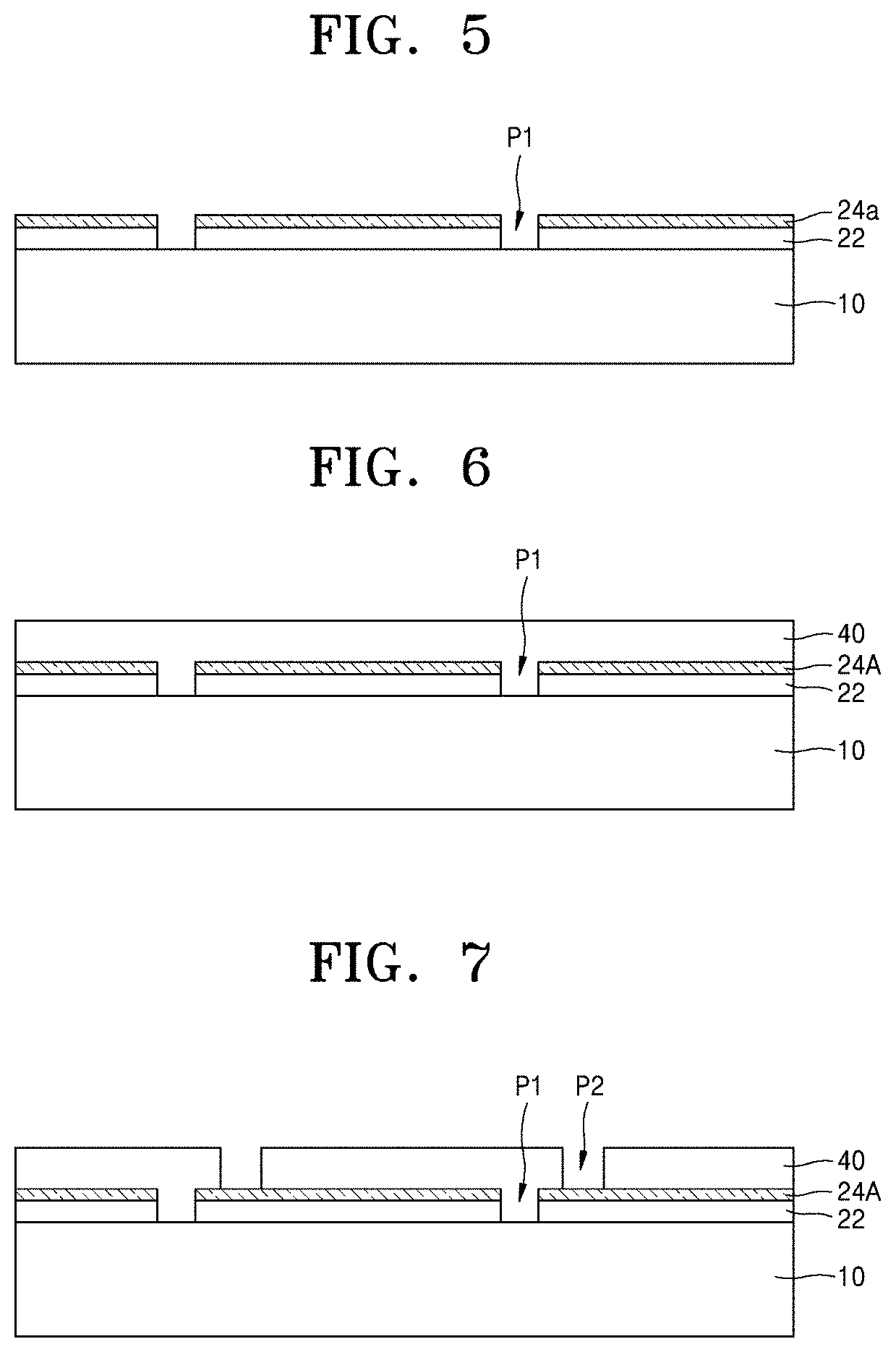
[0040]Hereinafter, the present invention will be described in detail by explaining embodiments of the invention with reference to the attached drawings. The invention may, however, be embodied in many different forms and should not be construed as being limited to the embodiments set forth herein; rather, these embodiments are provided so that this disclosure will be thorough and complete, and will fully convey the concept of the invention to one of ordinary skill in the art.

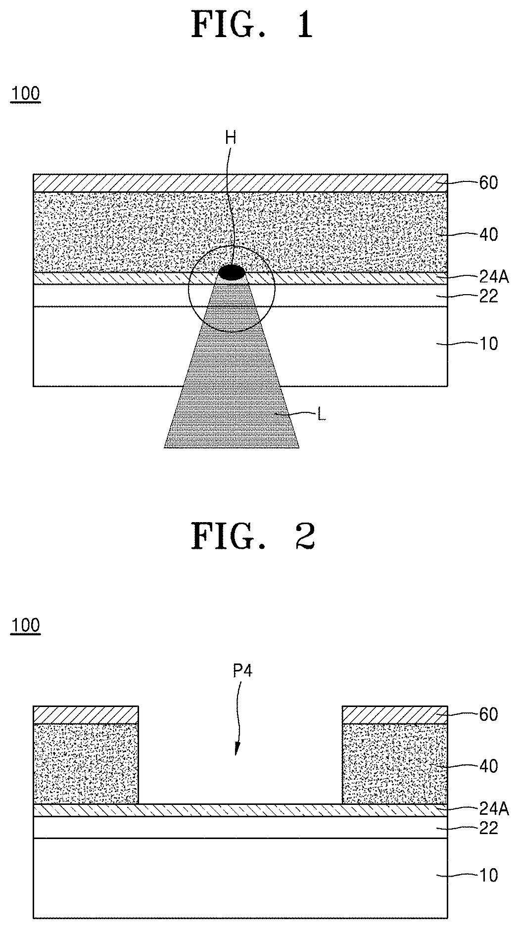
[0041]FIGS. 1 and 2 are cross-sectional views showing a structure of a see-through thin film solar cell 100 and a process of forming a fourth laser scribing pattern P4, according to an embodiment of the present invention.

[0042]Referring to FIG. 1, the see-through thin film solar cell 100 before forming the fourth laser scribing pattern P4 has a structure in which a first back electrode 22, a second back electrode 24A, an absorber layer 40, and a transparent electrode layer 60 are sequentially laminated on a firs...


PUM


Abstract

Provided is a see-through thin film solar cell module including a transparent substrate, a first back electrode deposited on a first surface of the transparent substrate, a second back electrode deposited on the first back electrode and including a MoSe2 layer, an absorber layer deposited on the second back electrode and including selenium (Se) or sulfur (S), and a laser scribing pattern formed by partially removing the absorber layer.

Description

CROSS-REFERENCE TO RELATED PATENT APPLICATION[0001]This application claims the benefit of Korean Patent Application No. 10-2020-0164370, filed on Nov. 30, 2020, in the Korean Intellectual Property Office, the disclosure of which is incorporated herein in its entirety by reference.BACKGROUND OF THE INVENTION1. Field of the Invention[0002]The present invention relates to a thin film solar cell module and a method of manufacturing the same and, more particularly, to a see-through chalcogenide thin film solar cell module having high transmittance, and a method of manufacturing the same.2. Description of the Related Art[0003]Chalcogenide thin film solar cells have excellent photovoltaic performance close to that of crystalline silicon solar cells, e.g., a photovoltaic efficiency of 23.4% in a Cu(In,Ga)(Se,S)2 absorber layer. In addition, based on light weights, the chalcogenide thin film solar cells attract much attention as a next-generation energy technology applicable to various envir...

Claims


Application Information

Patent Timeline
IPC IPC(8): H01L31/032H01L31/18H01L31/0224H01L31/0463
CPCH01L31/0322H01L31/0463H01L31/022441H01L31/1884H01L31/0468H01L31/0749H01L31/022425H01L31/0445H01L31/055H01L31/022466
Inventor JEONG, JEUNG-HYUNKIM, GEE YEONGYU, HYEONGGEUNKIM, WON MOKLEE, HYUNJAE
Owner KOREA INST OF SCI & TECH
Learn More