

Polishing pad sheet, polishing pad, and method for manufacturing semiconductor device
a technology for polishing pads and semiconductor devices, applied in the direction of polishing compositions, manufacturing tools, grinding machine components, etc., can solve the problems of reducing the size of individual chips, increasing the complexity and finer of the pattern of each layer, and achieving high durability, stable polishing process, and appropriate elasticity
- Summary
- Abstract
- Description
- Claims
- Application Information
AI Technical Summary
Benefits of technology
Problems solved by technology
Method used
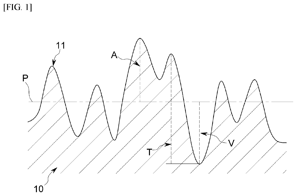
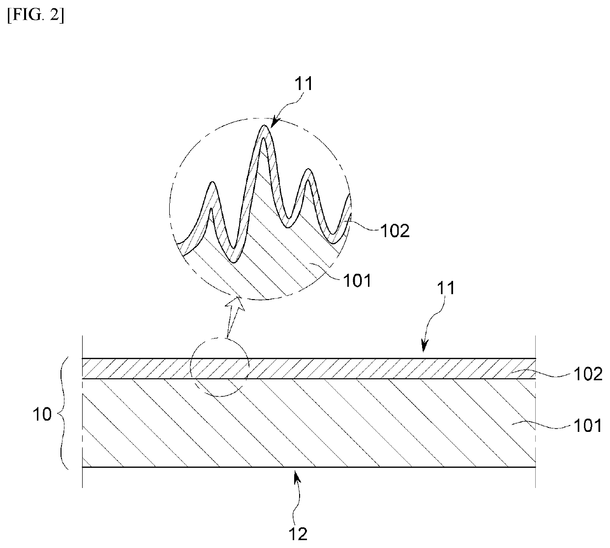
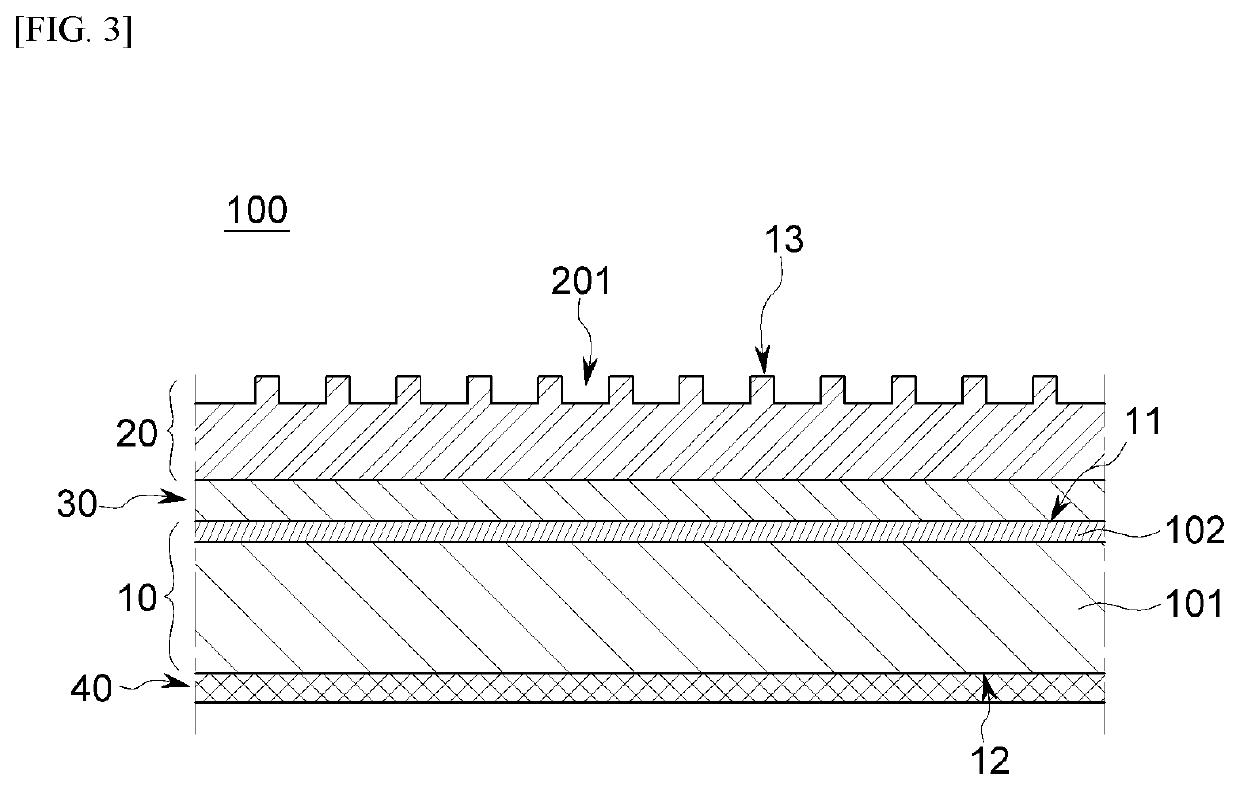
Image

Examples
experimental example 1
Properties of Polishing Layers
[0188]For each polishing layer, after a sample having a size of 5 cm (width)×5 cm (length)×2 mm (thickness) was cut and stored at a temperature of 25° C. for 12 hours, Shore D hardness was measured using a durometer.
[0189](2) Tensile Strength
[0190]For each polishing layer, a sample having a size of 4 cm (width)×1 cm (length)×2 mm (thickness) was cut, and the highest strength value just before breaking of the polishing pad was measured at a speed of 50 mm / min using a universal testing machine (UTM).
[0191](3) Elongation
[0192]For each polishing layer, after cutting a sample having a size of 4 cm (width)×1 cm (length)×2 mm (thickness) and measuring the maximum amount of deformation just before breaking of the polishing pad at a speed of 50 mm / min using a universal testing machine (UTM), the ratio of the maximum amount of deformation to the initial length was expressed as a percentage (%).
[0193](4) Density
[0194]For each polishing ...
experimental example 2
Properties of Polishing Pad Sheets
[0195](1) Hardness (Asker C)
[0196]For each polishing pad sheet, after a sample having a size of 5 cm (width)×5 cm (length)×2 mm (thickness) was cut and stored at a temperature of 25° C. for 12 hours, Asker C hardness was measured using a durometer.
[0197](2) Density
[0198]For each polishing pad sheet, after a sample having a size of 2 cm (width)×5 cm (length)×2 mm (thickness) was cut and stored at a temperature of 25° C. for 12 hours, the density was measured using a hydrometer.
[0199](3) Compressibility
[0200]For each polishing pad sheet, a compressibility (%) was derived using the equation of (D1−D2) / D1×100 by collecting a specimen measuring 25 mm in width and length each, measuring a dial gauge in no-load condition, and then pressing with a standard weight of 85 g to measure the first thickness (D1) when 30 seconds had elapsed, and by setting up a pressure condition in which 800 g of a weight was added to the standard weight and measuring the second ...
experimental example 3
Properties and Performance of Polishing Pads
[0203](1) Compressibility
[0204]For each polishing pad, a compressibility (%) was derived using the equation of (D1−D2) / D1×100 by collecting a specimen measuring 25 mm in width and length each, measuring a dial gauge in no-load condition, and then pressing with a standard weight of 85 g to measure the first thickness (D1) when 30 seconds had elapsed, and by setting up a pressure condition in which 800 g of a weight was added to the standard weight and measuring the second thickness (D2) when 3 minutes had elapsed.
[0205](2) Interfacial Adhesive Force
[0206]For each polishing pad, the interfacial adhesive force between each polishing layer and the cushion layer derived from each polishing pad sheet was measured by an 180 degree peel strength method using a universal testing machine (UTM) apparatus. At this time, the specimen was cut to a size of 25 mm (width)×300 mm (length), and the grip position was positioned to have a margin of about 50 mm...
PUM
 Abstract
Description
Claims
Application Information