Semiconductor device
- Summary
- Abstract
- Description
- Claims
- Application Information
AI Technical Summary
Benefits of technology
Problems solved by technology
Method used
Image

Examples
first embodiment
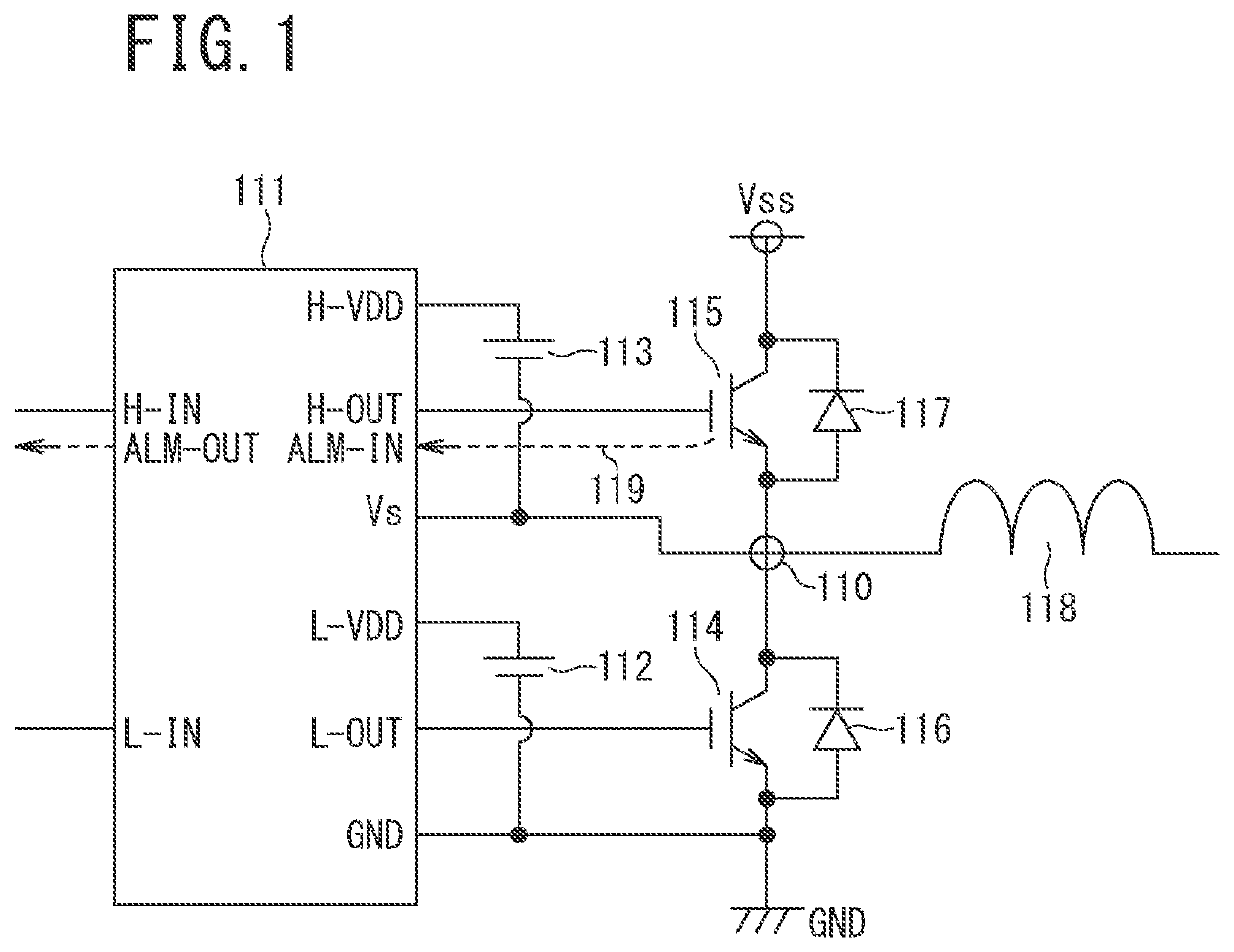
[0049]A semiconductor device (a semiconductor integrated circuit) according to a first embodiment of the present invention is illustrated below with a high-voltage integrated circuit (HVIC) of a self-shielding system. FIG. 1 illustrates a connection example between a HVIC 111 that is the semiconductor device according to the first embodiment of the present invention and IGBTs 114 and 115 that are switching power devices (switching elements) of a power conversion device such as an inverter driven by the HVIC 111. The switching elements of the power conversion device are not limited to the IGBTs 114 and 115, and may be other switching elements such as MOSFETs.
[0050]The IGBTs 114 and 115 are connected in series to implement a half bridge. The IGBTs 114 and 115 are connected antiparallel to freewheeling diodes (FWD) 116 and 117. An emitter of the IGBT 114 is connected to a ground potential (GND potential). A collector of the IGBT 115 is connected to a Vss potential on a high-potential s...
second embodiment
[0096]FIG. 11 is a plan view illustrating a main part of a semiconductor device (HVIC) according to a second embodiment of the present invention, and FIG. 12 is a cross-sectional view including the high-voltage n-channel MOSFET 41a as viewed from direction A-A′ in FIG. 11. The HVIC according to the second embodiment of the present invention illustrated in FIG. 11 and FIG. 12 differs from the semiconductor device according to the first embodiment of the present invention illustrated in FIG. 3 in that a contact of a pickup region (62a, 64), among pickup regions (62a, 64), 62b, 62c, and 62d of the H-VDD potential, adjacent to the drain region of the respective high-voltage re-channel MOSFETs 41a and 41b is a universal contact region.
[0097]As illustrated in FIG. 11 and FIG. 12, the pickup region (62a, 64) includes an n+-type pickup region 62a and p+-type contact regions 64 alternately arranged in contact with each other along the surface of the p-type semiconductor layer 1 so as to comp...
third embodiment
[0100]FIG. 13 is a plan view illustrating a main part of a semiconductor device (HVIC) according to a third embodiment of the present invention, and FIG. 14 is a cross-sectional view including the high-voltage n-channel MOSFET 41a as viewed from direction A-A′ in FIG. 13. The HVIC according to the third embodiment of the present invention illustrated in FIG. 13 and FIG. 14 differs from the semiconductor device according to the second embodiment of the present invention illustrated in FIG. 11 in that the drain region 52 of the respective high-voltage n-channel MOSFETs 41a and 41b is not the universal contact region.
[0101]The semiconductor device according to the third embodiment of the present invention is provided with the pickup region (62a, 64) of the H-VDD potential that is the universal contact region adjacent to the drain region 52 of the respective high-voltage n-channel MOSFETs 41a and 41b, so as to reduce the number of the hole carriers penetrating through the p-type junctio...
PUM
 Abstract
Description
Claims
Application Information
 - Generate Ideas
- Intellectual Property
- Life Sciences
- Materials
- Tech Scout
- Unparalleled Data Quality
- Higher Quality Content
- 60% Fewer Hallucinations
Browse by: Latest US Patents, China's latest patents, Technical Efficacy Thesaurus, Application Domain, Technology Topic, Popular Technical Reports.
© 2025 PatSnap. All rights reserved.Legal|Privacy policy|Modern Slavery Act Transparency Statement|Sitemap|About US| Contact US: help@patsnap.com