Method for manufacturing a radar sensor

a radar sensor and manufacturing method technology, applied in the direction of instruments, waveguides, semiconductor/solid-state device details, etc., can solve the problem of surface tension in solder, and achieve the effect of compact radar sensor, reduced manufacturing costs, and high packing density

Pending Publication Date: 2022-06-23
ROBERT BOSCH GMBH
View PDF0 Cites 0 Cited by
  • Summary
  • Abstract
  • Description
  • Claims
  • Application Information

AI Technical Summary

Benefits of technology

[0026]In accordance with an example embodiment of the present invention, the radar transceiver may essentially be mounted in two different variants at a surface of the circuit board. In one variant, the waveguide structure and the radar transceiver may be situated on different surfaces of the circuit board. The radar transceiver is preferably situated on the surface situated opposite the waveguide structure. The radar signal is then fed into the waveguide channel through the circuit board. For this purpose, waveguide transitions, coupling structures and/or hard-wired feeding using a metallized via may be provided. Since a circuit board is typically relatively thin, a short, direct coupling between the radar transceiver and the waveguide structure is possible. Further surface-mounted devices (SMDs) are preferably situated on the same surface as the radar transceiver. In this way, a one-sided mounting process is sufficient, by which the manufacturing costs are reduced. In addition, the circuit board is only heated on one side, and a heat conducting element may be provided on this side. In connection with the above-described modular units, additionally the advantage arises that the modular units of the waveguide structures may be situated and connected on the entire surface since no further components are provided on this surface. Moreover, an optical quality control of the SMDs and, above all, of the solder spots may be carried out from one side. Purely in principle, the further SMDs may also be situated at other, for example lateral, surfaces or at the same surface as the waveguide structure, and, if necessary, also beneath the waveguide structure.
[0027]In another variant, the waveguide structure and the radar transceiver may be situated on the same surface of the circuit boar

Problems solved by technology

Moreover, the waveguide antenna has to be attached with the aid of screws or glued to the circuit board in a complex process dur

Method used


Image

  • Method for manufacturing a radar sensor
  • Method for manufacturing a radar sensor
  • Method for manufacturing a radar sensor

Examples


Embodiment Construction

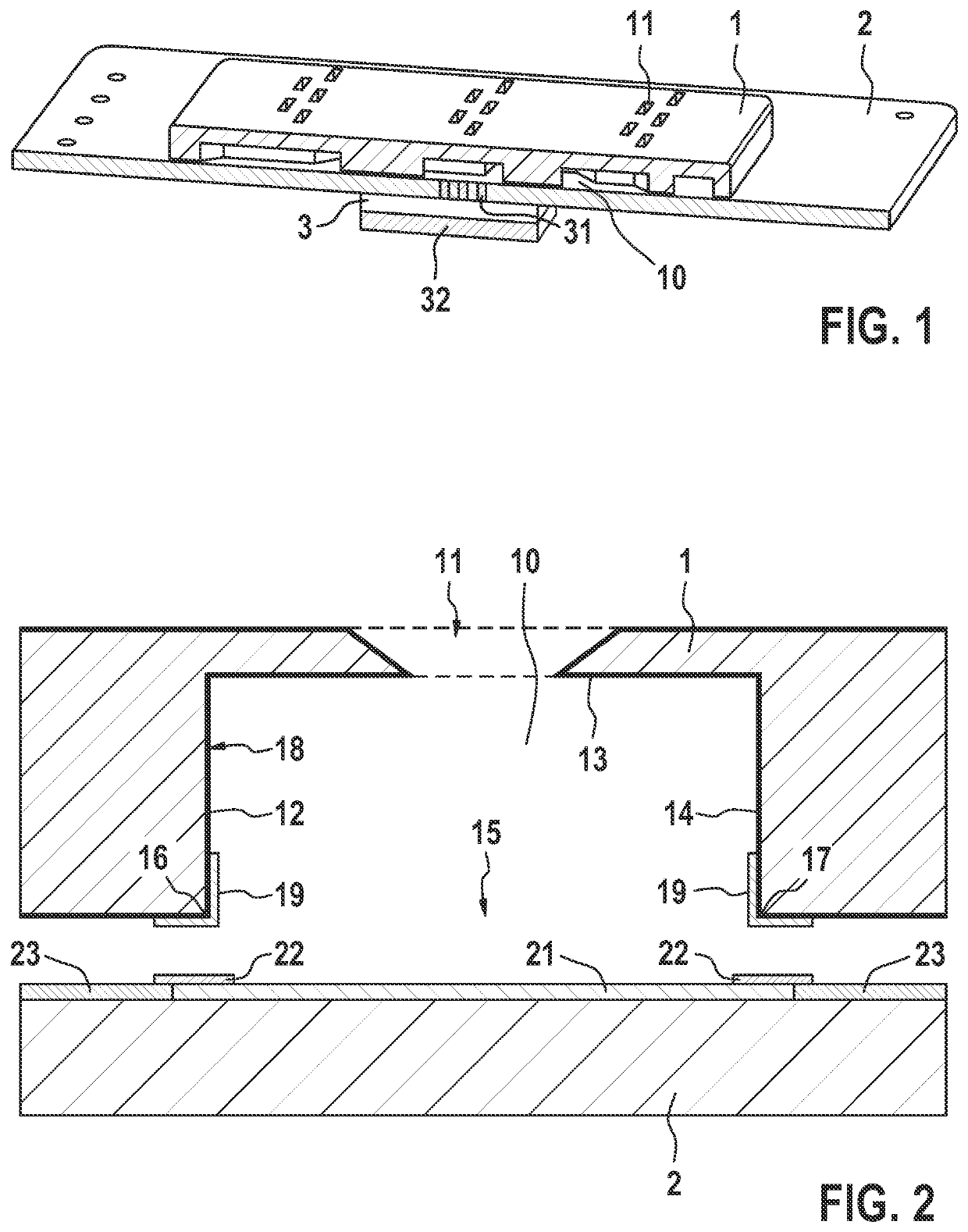
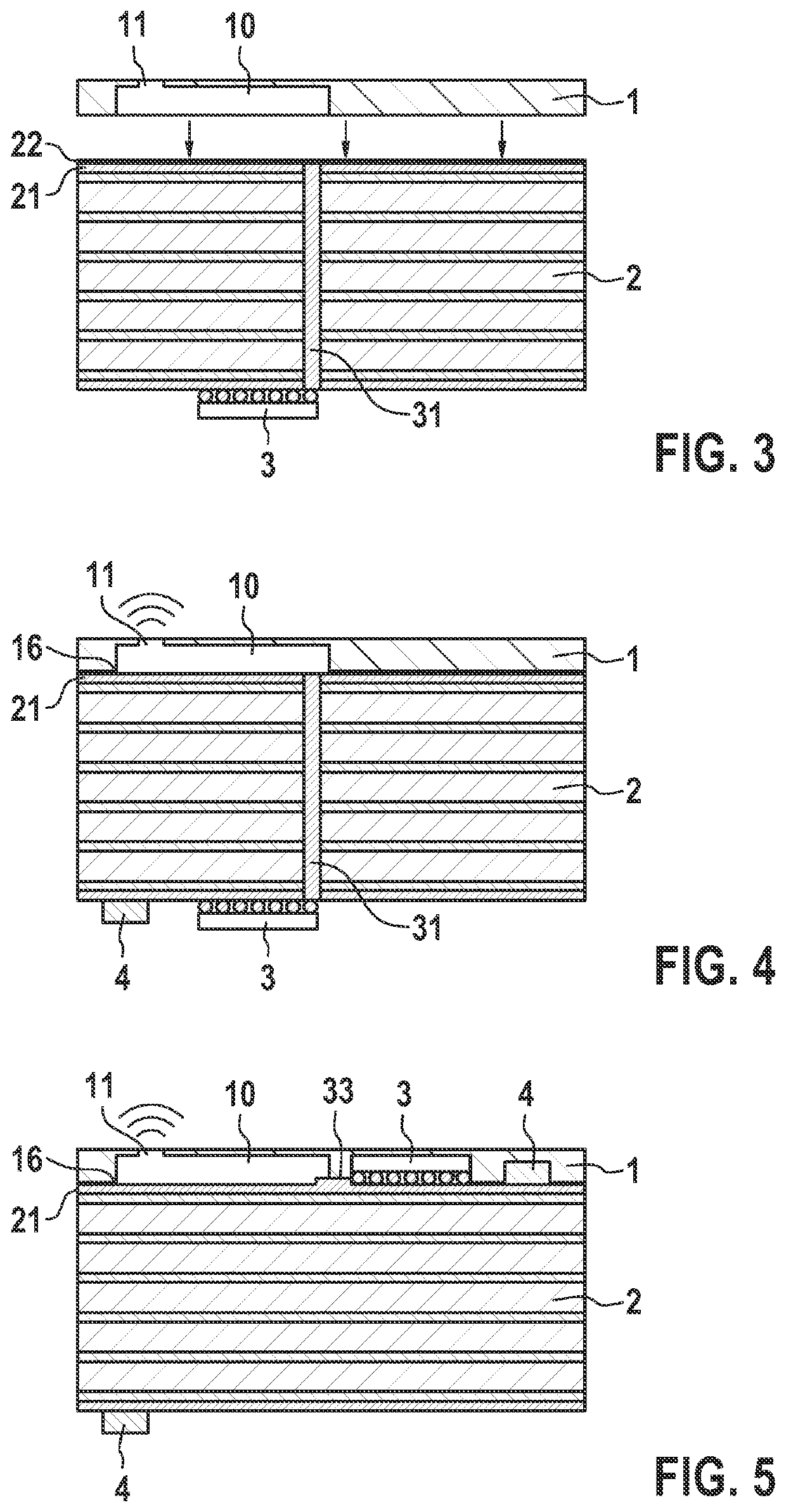
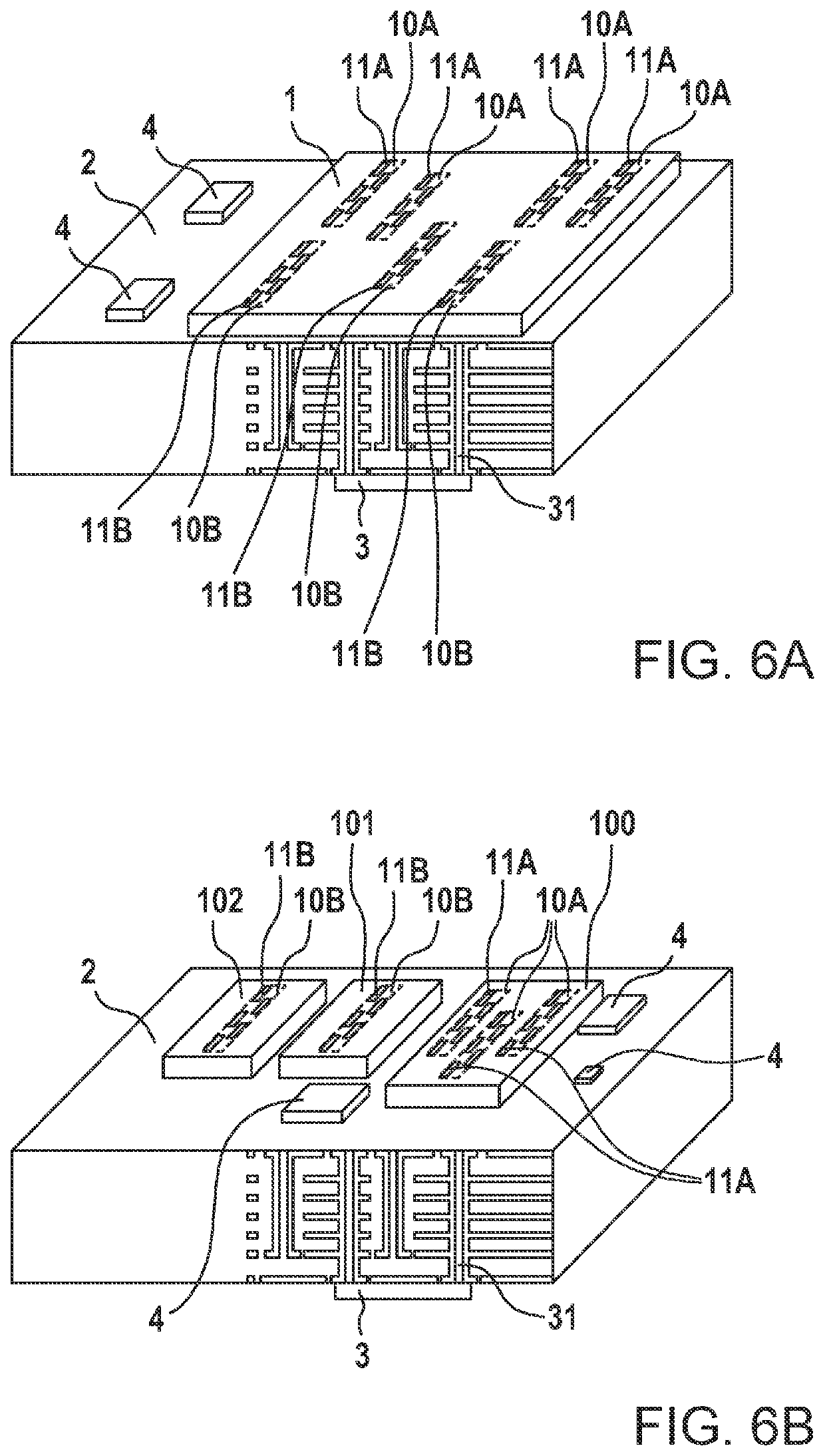
[0038]FIG. 1 shows a cut isometric view of a radar sensor according to one exemplary embodiment of the present invention. The radar sensor includes a waveguide structure 1 made of plastic, which is designed in the shape of a block, and a circuit board 2, which is made up of multiple layers (multi-layer circuit board) and was manufactured with the aid of standard FR4 technology. Waveguide structure 1 was connected to a surface of circuit board 2 (hereafter referred to as the upper side) using a soldering process, which is described in detail hereafter. Waveguide structure 1 includes multiple waveguide channels 10 having a rectangular cross-section, which together with the surface of circuit board 2 serve as waveguides for radar signals. In this way, an antenna structure for the radar sensor is formed. For a detailed description of waveguide channels 10, reference is made to the following description. Multiple slot-shaped openings are formed in waveguide structure 1, which connect wav...


PUM


Abstract

A method for manufacturing a radar sensor. In the method, a circuit board is provided. A surface of the circuit board is equipped with a radar transceiver. A waveguide structure made of plastic material is provided. Waveguide channels including at least one metallic conductively coated side wall in the waveguide structure and an open side are formed. The waveguide structure is soldered to a surface of the circuit board, the open side being oriented in the direction of the circuit board.

Description

CROSS REFERENCE[0001]The present application claims the benefit under 35 U.S.C. § 119 of German patent Application No. DE 102020216362.6 filed on Dec. 21, 2020, which is expressly incorporated herein by reference in its entirety.FIELD[0002]The present invention relates to a method for manufacturing a radar sensor including a waveguide structure, which is soldered onto a circuit board, and to a corresponding radar sensor.BACKGROUND INFORMATION[0003]Today, radar sensors are used in vehicles, for example, to implement comfort functions, such as e.g., adaptive cruise control, and safety functions, such as e.g., emergency braking assistants. Radar sensors directly measure the relevant physical variables, such as e.g., the distance from a target, without being dependent on an interpretation of images, as takes place, e.g., with an optical camera.[0004]Radar sensors emit high-frequency radar signals via an antenna structure in the direction of an object and usually receive the radar signal...

Claims


Application Information

Patent Timeline
IPC IPC(8): G01S7/03H01Q1/22H01L23/66G02B6/122
CPCG01S7/032H01Q1/2283H01Q23/00G02B6/1228H01L2223/6677H01L23/66H01P3/12H01Q21/28G01S7/03H01L2223/6627H01L2223/6683H01L2924/19105H01L2224/16227G01S7/027G01S7/028G01S13/931
Inventor HOLLAENDER, CHRISTIANBAUR, KLAUSHIMMELSTOSS, ARMINKLETT, GUSTAVSCHOOR, MICHAELPHAM, MINH NHAT
Owner ROBERT BOSCH GMBH
Why Eureka
Try Eureka