Photoresist resolution capabilities by copper electroplating anisotropically

Pending Publication Date: 2022-07-07
ROHM & HAAS ELECTRONICS MATERIALS LLC
View PDF5 Cites 0 Cited by
  • Summary
  • Abstract
  • Description
  • Claims
  • Application Information

AI Technical Summary

Benefits of technology

[0012]The methods of the present invention enable copper electroplating anisotropically of features having different shapes and sizes, which are maintained even when electroplated layer thickness is substantially higher than the thickness of the photoresist. The methods of the present invention enable formation of

Problems solved by technology

This multidirectional expansion compromises the integrity of the circuit, for example, by joining adjacent features and creating circuit shorts that render the whole architecture useless.
These trends, borne out of the natural limitations of plating technologies,

Method used


Image

  • Photoresist resolution capabilities by copper electroplating anisotropically
  • Photoresist resolution capabilities by copper electroplating anisotropically
  • Photoresist resolution capabilities by copper electroplating anisotropically

Examples


examples 1-2

Plating Height Levelling on 3-mercapto-propylsulfonic Acid Sodium Salt Activated 1-100 μm Fine-line Pattern with Highly Anisotropic Bath 3, vs. No Activation with Isotropic Bath 1

[0056]The following two copper electroplating baths were prepared:

Plating Bath 1 (Isotropic Bath):

[0057]50 g / L Cu(II) ion[0058]100 g / L H2SO4 [0059]50 ppm Chloride ion[0060]5 ppm Bis-Sodium-Sulfopropyl-Disulfide[0061]2 g / L EO-PO random copolymer with average MW 1,100 and hydroxyl end groups 5 ppm reaction product of epichlorohydrin and imidazole

Plating Bath 2 (Anisotropic Bath):

[0062]50 g / L Cu(II) ion[0063]100 g / L H2SO4[0064]50 ppm Chloride ion[0065]40 ppm Bis-Sodium-Sulfopropyl-Disulfide[0066]2 g / L EO-PO random copolymer with average MW 1,100 and hydroxyl end groups[0067]1 ppm reaction product of butyldiglycidylether, imidazole and phenylimidazole

Plating Bath 3 (Anisotropic Bath):

[0068]50 g / L Cu(II) ion[0069]100 g / L H2SO4 [0070]50 ppm Chloride ion[0071]20 ppm Bis-Sodium-Sulfopropyl-Disulfide[0072]2 g / L Diam...

examples 3-6

Line Broadening on MES Activated 1-100 μm Fine-line Pattern with Highly Surface Reactive Bath 2, vs. No Activation with Non-surface Reactive Bath 1

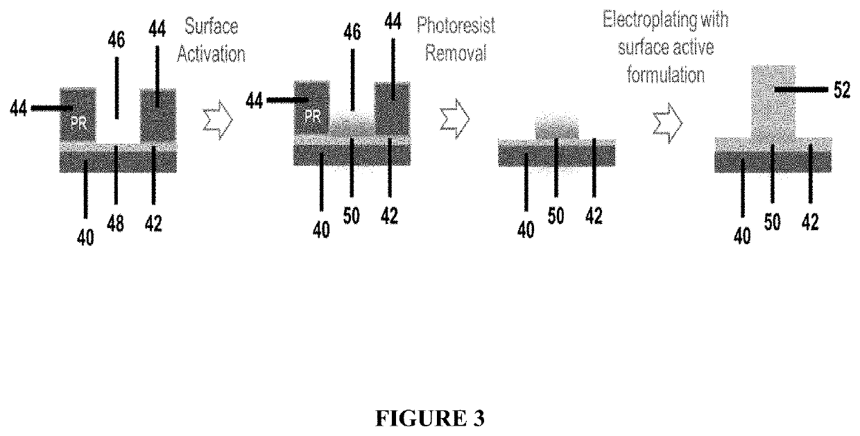
[0075]A silicon wafer coated with a 20 nm Ti adhesion layer and a 200 nm conductive Cu seed was laminated with a PR layer with a thickness of 3 μm. A fine line pattern was built on the PR layer to contain a series of trenches ranging from 1 to 100 μm in width. These trenches were then plated to a target height of 4.5 μm using either Plating Bath 1 or Plating Bath 3. In each case, the samples were either wetted with DI water prior to plating, or they were first immersed in a pH 0.7 solution of 4 g / L MES in water and then rinsed with DI water prior to plating. In all cases, electroplating was carried out at 2 ASD with a cathode rotation rate of 50 rpm. Following plating, the PR was removed in a PR stripper bath to yield a pattern of fine lines. The sample was then exposed to a seed etch solution to remove the remaining conductive seed that ...

examples 7-10

Line Broadening on MES Activated 1-100 μm Fine-line Pattern with Highly Surface Reactive Bath 3, vs. No Activation with Non-surface Reactive Bath 1

[0076]A silicon wafer coated with a 20 nm Ti adhesion layer and a 200 nm conductive Cu seed was laminated with a PR layer with a thickness of 3 μm. A fine line pattern was built on the PR layer to contain a series of 100 μ-wide trenches. The substrate was then plated to a target height of 36 μm using either Plating Bath 1 or Plating Bath 3. The sample plated with Plating Bath 1 was wetted with DI water prior to plating. The sample plated with Plating Bath 3 was first immersed in a pH 0.7 solution of 4 g / L MES in water and then rinsed with DI water prior to plating. In both cases, electroplating was carried out at 2 ASD with a cathode rotation rate of 50 rpm. Following plating, the PR was removed in a PR stripper bath to yield a pattern of fine lines. The samples were then imaged via SEM. Table 3 show that the sample plated with Plating Ba...


PUM

PropertyMeasurementUnit
Angleaaaaaaaaaa
Angleaaaaaaaaaa
Heightaaaaaaaaaa

Abstract

Features of substrates are copper electroplated by a method which involves copper electroplating selectively deposited seed layers or seed layers of photoresist defined features with a copper electroplating composition containing select suppressor compounds and select leveler compounds which enable anisotropic plating. Optionally, the seed layers can be treated with an aqueous solution of sulfur containing accelerators prior to copper electroplating.

Description

FIELD OF THE INVENTION[0001]The present invention is directed to a method of improving photoresist resolution capabilities by copper electroplating anisotropically of photoresist defined features. More specifically, the present invention is directed to a method of improving photoresist resolution capabilities by copper electroplating anisotropically of photoresist defined features by copper electroplating anisotropically seed layers of the photoresist defined features of the substrate with an aqueous copper electroplating composition containing select suppressors and select leveler compounds which enable copper electroplating anisotropically, wherein the seed layers of the photoresist defined features can be optionally treated with a solution of sulfur containing accelerator compounds prior to copper electroplating anisotropically of the seed layers.BACKGROUND OF THE INVENTION[0002]Packaging and interconnection of electronic components relies on the ability to create a circuit patte...

Claims


Application Information

Patent Timeline
IPC IPC(8): C25D5/00C25D7/12C25D3/38G03F7/20C25D5/02
CPCC25D5/605C25D7/123C25D5/02G03F7/20C25D3/38C25D21/14C25D21/12G03F7/40C25D5/617C25D7/00C25D5/022H05K3/241H05K3/107
Inventor LIFSCHITZ ARRIBIO, ALEJO M.ZIELINSKI, ALEXANDERHAMMOODI, SAMERLACHOWSKI, JOSEPH F.GALLAGHER, MICHAEL K.WILLIAMSON, CURTISPRANGE, JONATHAN D.
Owner ROHM & HAAS ELECTRONICS MATERIALS LLC
Why Eureka
Try Eureka