Semiconductor component on a heat pipe

a technology of semiconductors and heat pipes, applied in the direction of electrical equipment construction details, indirect heat exchangers, lighting and heating apparatus, etc., can solve the problems of increased internal pressure, deformation or explosion of heat pipes, and the inability to apply temperature-sensitive joining methods

Pending Publication Date: 2022-07-14
SIEMENS AG
View PDF0 Cites 0 Cited by
  • Summary
  • Abstract
  • Description
  • Claims
  • Application Information

AI Technical Summary

Benefits of technology

[0013]The present embodiments may obviate one or more of the drawbacks or limitations in the related art. For example, a thermal conductivity between power semiconductor components and a heat pipe in a power module is improved.
[0025]In a development, the joining is soldering or sintering, where during sintering, the heat pipe and the power semiconductor component are located in a pocket that presses the power semiconductor component onto the heat pipe by increasing the external pressure.

Problems solved by technology

This increases the internal pressure of the heat pipe, with the result that it is possible for deformation or explosion of the heat pipe to occur.
For example, in the case of flat heat pipes (e.g., vapor chambers), joining methods that are subjected to temperature are therefore not possible because of the geometry.
The thermal and the electrical conductivity between a heat source and a heat pipe is thus not optimal according to the prior art.
The attachment of power semiconductor components to heat pipes by conventional joining methods of power electronics (e.g., soldering, silver sintering) that permit a high thermal conductivity between semiconductor and heat pipe is therefore not possible, as explained above.
In the joining method of silver sintering under pressure, a further problem is added.
This is not possible when joining to heat pipes, since the heat pipe will be deformed and destroyed as a result.
In addition, the available layer thicknesses of the copper metallizations of such substrates are less than 1 mm, which likewise limits the lateral thermal conduction.
This leads to the use of large heat sinks with extremely long and heavy cooling fins.
The attachment of power semiconductor components to heat pipes using conventional joining methods of power electronics (e.g., soldering, silver sintering) that permit high thermal conductivity between semiconductor and heat pipe has not been possible until now.

Method used


Image

  • Semiconductor component on a heat pipe
  • Semiconductor component on a heat pipe
  • Semiconductor component on a heat pipe

Examples


Embodiment Construction

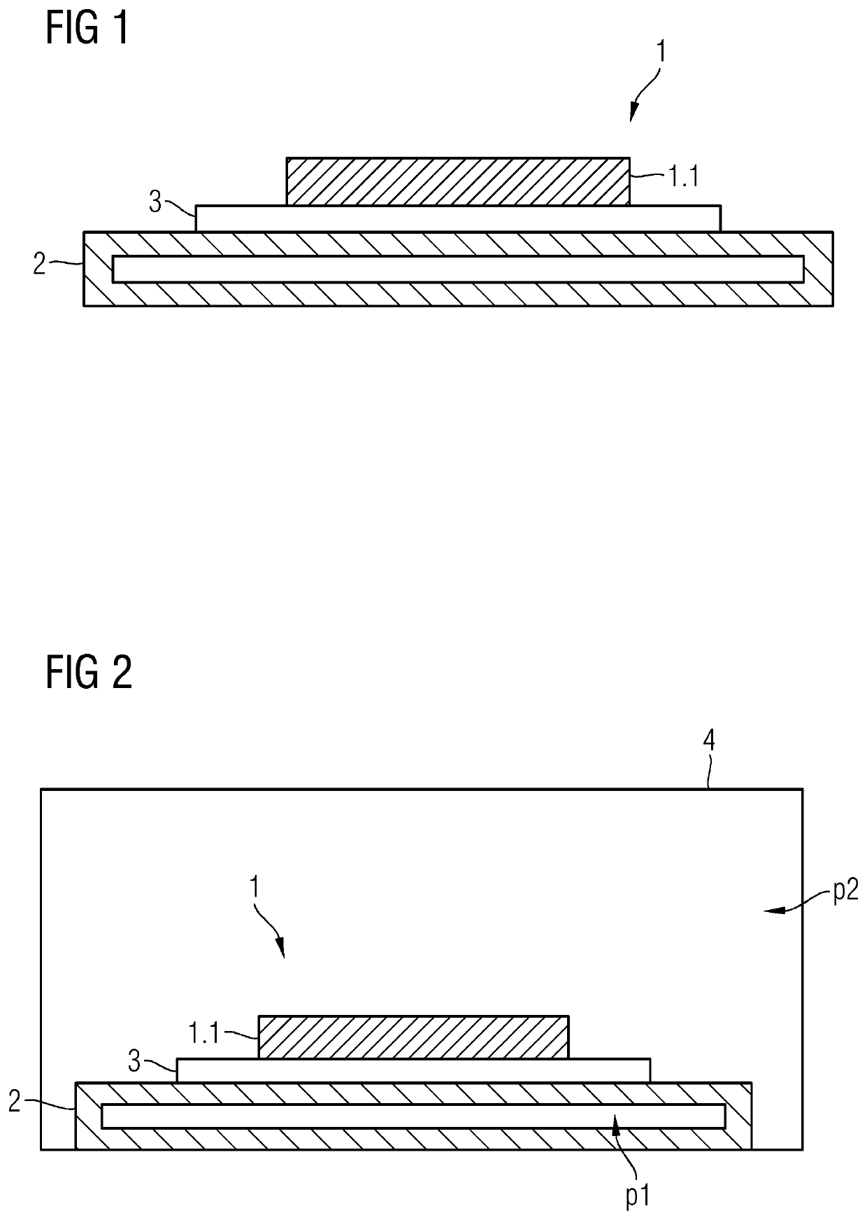
[0042]FIG. 1 shows a side view of parts of a power module 1 of a converter according to the prior art. A plurality of power semiconductor components 1.1 (only one is visible) are joined to a heat pipe 2 with the aid of an integral connection 3 (e.g., adhesive). The heat pipe 2 is used for effective heat dissipation of a power loss of the power semiconductor components 1.1. The heat pipe 2 is, for example, filled with water.

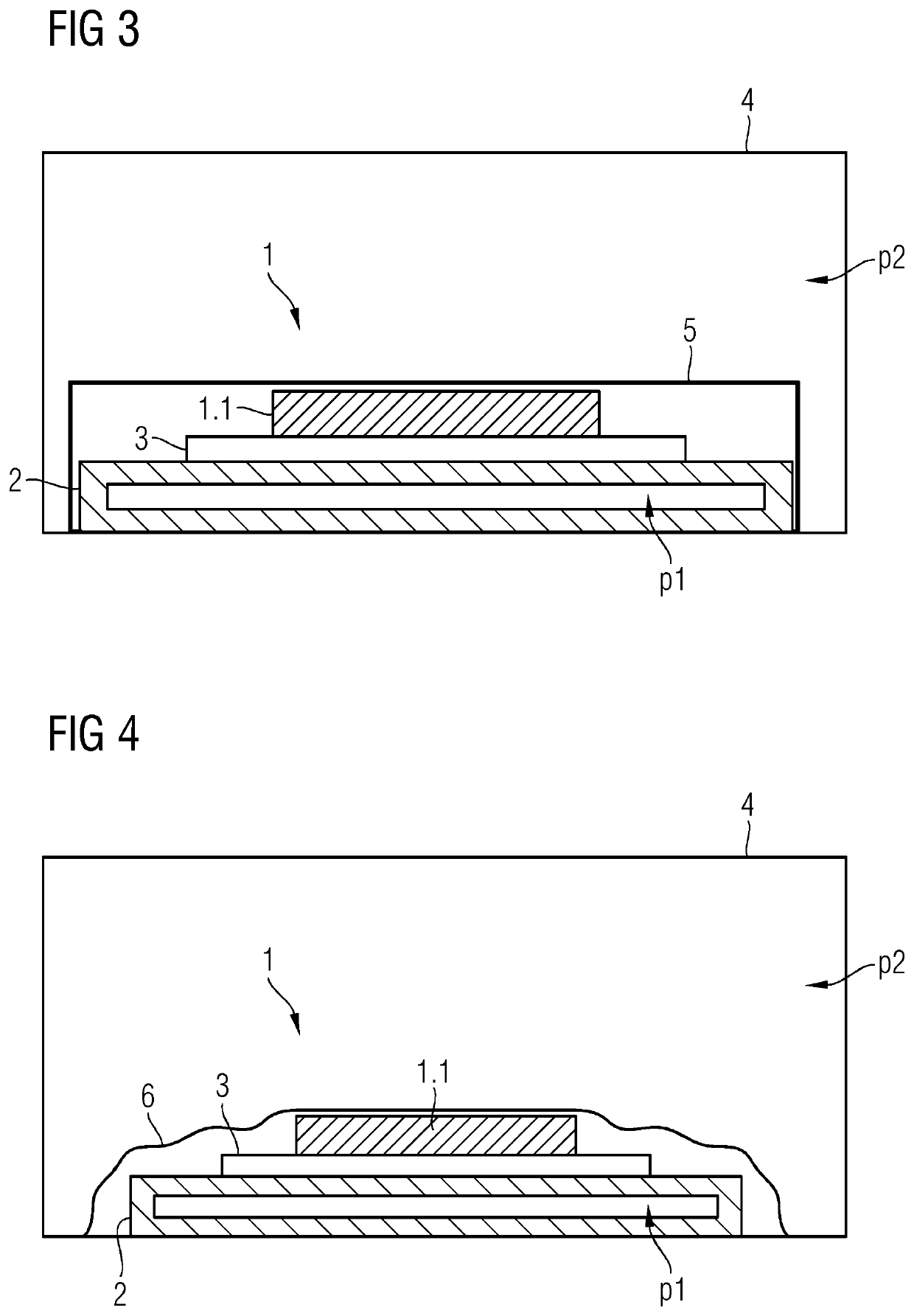
[0043]FIG. 2 shows a view of a device for soldering power semiconductor components 1.1 of a power module 1 to a water-filled heat pipe 2. The integral connection 3 is produced by a solder. In order that an internal pressure p1 in an interior of the heat pipe 2 during soldering does not cause the heat pipe 2 to burst, the soldering operation is carried out in a pressure chamber 4 that builds up an external pressure p2. The external pressure p2 is automatically adjusted such that the internal pressure p1 is always approximately equal to the external pressure p2.

[004...


PUM


Abstract

The invention relates to a method for joining a power semiconductor component (1.1) to a heat pipe (2), wherein, during joining, the external pressure (p2) acting on the heat pipe (2) is changed proportionally to the internal pressure (p1) of the heat pipe (2), which internal pressure changes under heat during joining. The invention also relates to a device for carrying out the method, a power module, a converter and a vehicle.

Description

[0001]This application is the National Stage of International Application No. PCT / EP2020 / 060663, filed Apr. 16, 2020, which claims the benefit of German Patent Application No. DE 10 2019 206 896.0, filed May 13, 2019. The entire contents of these documents are hereby incorporated herein by reference.FIELD[0002]The present embodiments relate to joining a power semiconductor component to a heat pipe.BACKGROUND[0003]Since the power losses to be dissipated in power modules are produced only in a point-like manner in the power semiconductor component (e.g., chip area ˜1 cm2), the lateral heat conduction (e.g., “heat spreading”) within the power module plays a critical role in order to minimize the thermal resistance of the semiconductor or of the module for cooling. The higher the lateral heat conduction with a constant vertical heat conduction, the better is the utilization of the cooling area available.[0004]A very effective way of transporting heat laterally is represented by the use ...

Claims


Application Information

Patent Timeline
Patent Type & Authority Applications(United States)
IPC IPC(8): H05K7/20H01L23/427B64D33/08
CPCH05K7/20936B64D33/08H01L23/427H01L21/4882F28D15/0283F28D2021/0021F28D2021/0029F28F2275/04
Inventor WALTRICH, UWE
Owner SIEMENS AG
Why Eureka
Try Eureka