Laser processing method

a laser processing and laser technology, applied in the field of laser processing methods, can solve the problems of low-k material brittle like mica, local peeled organic films, and brittleness of low-k materials, and achieve the effect of suppressing the peeling of organic films

Pending Publication Date: 2022-09-15
DISCO CORP
View PDF0 Cites 0 Cited by
  • Summary
  • Abstract
  • Description
  • Claims
  • Application Information

AI Technical Summary

Benefits of technology

[0008]Preferably, in the blackening step, base parts of a Gaussian distribution of the pulsed laser beam applied to the organic films are modified to a vertical distribution, so that the pulsed laser beam of energy lower than the processing threshold value is prevented from being transmitted through the organic films and applied to the substrate.
[0009]The present invention produces an effect of being able to suppress the peeling of the organic films.

Problems solved by technology

The Low-k material is brittle like mica, and is peeled when cut by a cutting blade.
However, the interlayer insulating film as the Low-k material is transparent to the laser beam in these ultraviolet to visible light regions, and does not absorb the applied laser beam.
However, there is a problem in that, for example, the organic films are locally peeled as the laser beam is condensed in the silicon wafer and the silicon wafer sublimates.

Method used


Image

  • Laser processing method
  • Laser processing method
  • Laser processing method

Examples


Embodiment Construction

[0022]An embodiment of the present invention will hereinafter be described in detail with reference to the drawings. The present invention is not limited by contents described in the following embodiment. In addition, constituent elements described in the following include constituent elements readily conceivable by those skilled in the art and essentially identical constituent elements. Further, configurations described in the following can be combined with each other as appropriate. In addition, various omissions, replacements, or modifications of configurations can be performed without departing from the spirit of the present invention.

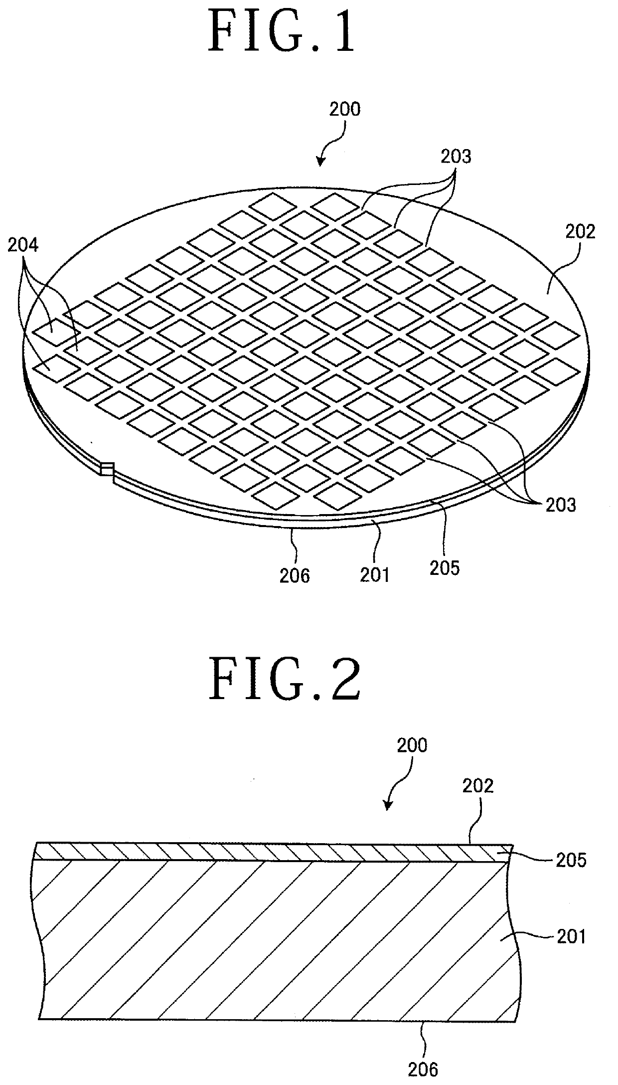
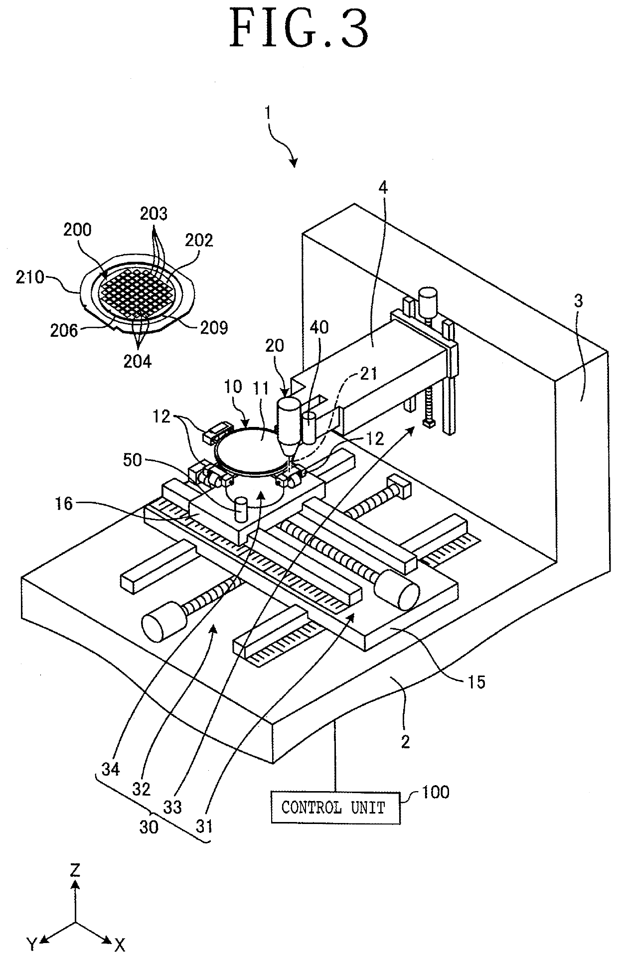
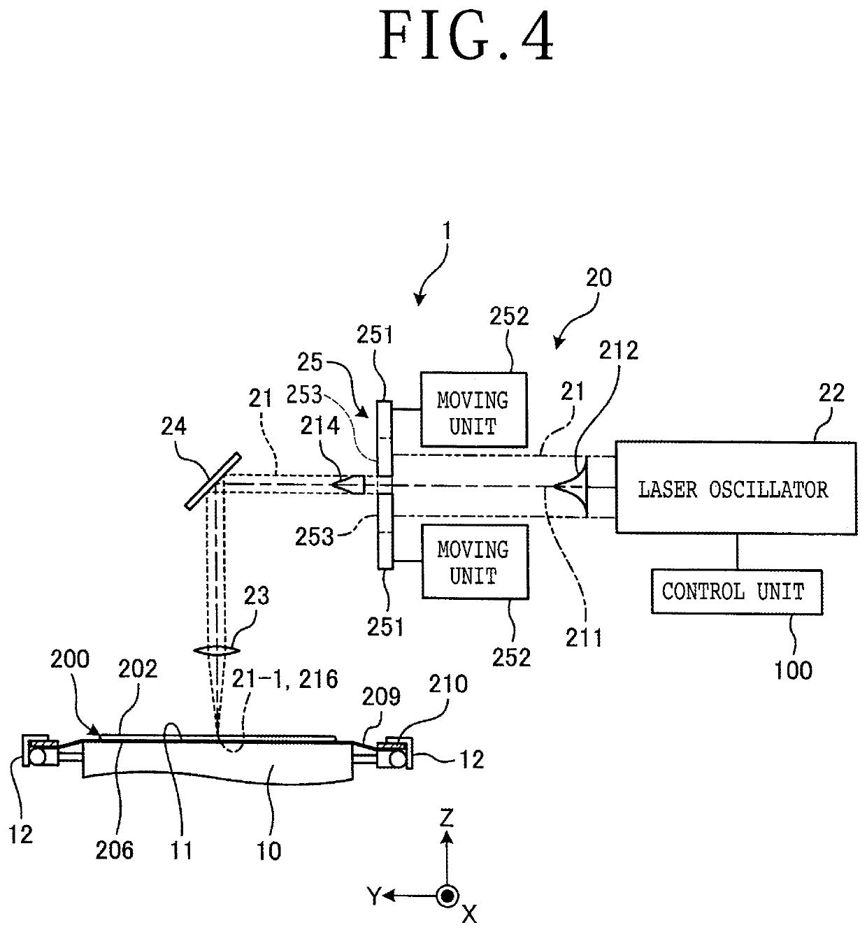
[0023]A laser processing method according to an embodiment of the present invention will be described with reference to the drawings. FIG. 1 is a perspective view of a wafer to be processed by the laser processing method according to the embodiment. FIG. 2 is a sectional view of principal parts of the wafer depicted in FIG. 1. FIG. 3 is a perspecti...


PUM

PropertyMeasurementUnit
wavelengthaaaaaaaaaa

Abstract

There is provided a laser processing method for performing laser processing on a wafer having a functional layer on a substrate. The laser processing method includes a blackening step of emitting a pulsed laser beam of a wavelength transparent to the functional layer from a laser oscillator and blackening the functional layer by irradiating the functional layer with the pulsed laser beam of energy equal to or higher than a processing threshold value at which the functional layer is processed such that an overlap ratio of the pulsed laser beam successively applied to the functional layer is equal to or more than 90% and less than 100%, and a groove processing step of forming a laser-processed groove by irradiating the blackened functional layer with the pulsed laser beam and making the blackened functional layer absorb the pulsed laser beam, after performing the blackening step.

Description

BACKGROUND OF THE INVENTIONField of the Invention[0001]The present invention relates to a laser processing method that performs laser processing on a wafer having organic films on a substrate.Description of the Related Art[0002]In recent years, in order to increase semiconductor device processing speed, there has been put to practical use a semiconductor wafer in which semiconductor devices are formed by laminating interlayer insulating films formed of an organic low dielectric constant material (what is generally called a Low-k material), the interlayer insulating film being a polyimide-based polymer film, a parylene-based polymer film, or the like, onto a silicon wafer together with a circuit layer, and thus organic films are laminated on the surface of a substrate formed of silicon (see Japanese Patent Laid-Open No. 2015-126054, for example).SUMMARY OF THE INVENTION[0003]The Low-k material is brittle like mica, and is peeled when cut by a cutting blade. Accordingly, as disclosed ...

Claims


Application Information

Patent Timeline
Patent Type & Authority Applications(United States)
IPC IPC(8): B23K26/0622B23K26/40B23K26/364B23K26/352
CPCB23K26/0622B23K26/40B23K26/364B23K26/352B23K2101/40C30B33/04C30B29/06B23K26/00B23K26/402B23K26/702B23K26/60B23K26/18B23K26/0823B23K26/0853B23K26/0869H01L21/31138
Inventor KIRIHARA, NAOTOSHIKANEKO, TAKAMASA
Owner DISCO CORP
Why Eureka
Try Eureka