Temperature sensor film, conductive film and method for producing same

a technology of temperature sensor and conductive film, which is applied in the direction of conductive layers on insulating supports, instruments, heat measurement, etc., can solve the problems of increased cost and complicated production process, and achieve the effect of high temperature measurement accuracy and large temperature coefficient of resistan

Pending Publication Date: 2022-11-03
NITTO DENKO CORP
View PDF0 Cites 0 Cited by
  • Summary
  • Abstract
  • Description
  • Claims
  • Application Information

AI Technical Summary

Benefits of technology

[0015]Since the interplanar spacing of the (111) plane in the nickel thin-film (lattice spacing of nickel) disposed on the resin film base is small, a temperature sensor film having a large temperature coefficient of resistance and high temperature measurement accuracy can be formed.

Problems solved by technology

In a case where temperatures at a plurality of locations in one plane are measured by a thermocouple, a chip thermistor, or the like, it is required to arrange the temperature sensor at each measurement point and connect the respective temperature sensors to a printed wiring board or the like, resulting in a complicated production process.
In addition, in order to measure an in-plane temperature distribution, it is required to arrange a large number of sensors on a substrate, which causes an increase in cost.

Method used


Image

  • Temperature sensor film, conductive film and method for producing same
  • Temperature sensor film, conductive film and method for producing same

Examples


example 1

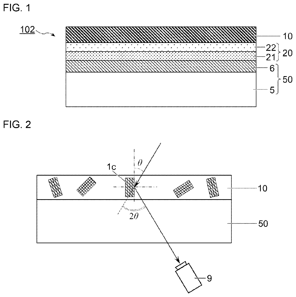
[0087]A roll of a polyethylene terephthalate (PET) film (“Lumirror 149UNS” manufactured by Toray Industries, arithmetic mean roughness Ra: 1.6 nm) having a thickness of 150 μm was set in a roll-to-roll sputtering apparatus, exhaustion was performed until a degree of ultimate vacuum in the sputtering apparatus reached 5.0×10⁻³ Pa, and then, a silicon thin-film having a thickness of 5 nm, a silicon oxide thin-film having a thickness of 10 nm, and a nickel thin-film having a thickness of 270 nm were sequentially deposited on the PET film at a substrate temperature of 150° C. by DC sputtering. A B-doped Si target was used to form a Si layer and a SiO2 layer. The Si layer was deposited by introducing argon as a sputtering gas under conditions of a pressure of 0.3 Pa and a power density of 1.0 W / cm2. The SiO2 layer was deposited by introducing oxygen as a reactive gas (O2 / Ar=0.12 / 1.0) in addition to argon as a sputtering gas under conditions of a pressure of 0.3 Pa and a power density of ...

example 2

[0088]The electroconductive film of Example 1 was heated in a hot air oven at 155° C. for 60 minutes to produce an electroconductive film.

example 3

[0092]The electroconductive film of Comparative Example 3 was heated in a hot air oven at 155° C. for 60 minutes to produce an electroconductive film.


PUM

PropertyMeasurementUnit
interplanar spacingaaaaaaaaaa
thicknessaaaaaaaaaa
thicknessaaaaaaaaaa

Abstract

Provided is a temperature sensor film comprising a metal-thin film patterned on a resin film substrate, and having high temperature measurement accuracy. A conductive film (102) that is used for producing a temperature sensor film has a nickel thin film (10) on one principal surface of a resin film substrate (50). It is preferable that the interplanar spacing of nickel (111) plane in the nickel thin-film is less than 0.2040 nm. The temperature sensor film is obtained by patterning the nickel thin film to form a temperature-measuring resistance part and a lead part connected to the temperature-measuring resistance part.

Description

TECHNICAL FIELD[0001]The present invention relates to a temperature sensor film including a patterned metal thin-film formed on a resin film base, an electroconductive film used in production of the temperature sensor film, and a method for producing the same.BACKGROUND ART[0002]A large number of temperature sensors are used in electronic devices. As the temperature sensor, a thermocouple or a chip thermistor is generally used. In a case where temperatures at a plurality of locations in one plane are measured by a thermocouple, a chip thermistor, or the like, it is required to arrange the temperature sensor at each measurement point and connect the respective temperature sensors to a printed wiring board or the like, resulting in a complicated production process. In addition, in order to measure an in-plane temperature distribution, it is required to arrange a large number of sensors on a substrate, which causes an increase in cost.[0003]Patent Document 1 proposes a temperature sens...

Claims


Application Information

Patent Timeline
Patent Type & Authority Applications(United States)
IPC IPC(8): G01K7/18
CPCG01K7/183G01K2007/163H01B5/14H01B1/02G01K7/22H01B13/00H01B13/0026G01K1/026G01K7/18C23C14/205C23C14/10G01K7/16G01K2217/00
Inventor YASUI, SATOSHIMIYAMOTO, KODAISHIBUYA, KATSUNORI
Owner NITTO DENKO CORP
Why Eureka
Try Eureka