Semiconductor device and method of fabricating the same

a semiconductor and semiconductor technology, applied in the field of semiconductor devices, can solve the problems of damage to the quantum well layer 203, difficult to obtain good crystal state and good electron state, and difficult to connect the quantum box 203 to external wirings

Inactive Publication Date: 2000-01-04
FUJITSU LTD
View PDF7 Cites 145 Cited by
  • Summary
  • Abstract
  • Description
  • Claims
  • Application Information

AI Technical Summary

Problems solved by technology

However, if the quantum box is formed by dry etching, the quantum well layer 203 is damaged due to dry etching.
As a result, it becomes difficult to obtain good crystal states and good electron states.
Therefore, it is not easy to connect the quantum box 203 to external wirings.
As has been stated above, the technique for forming the quantum dot by dry etching or selective growth may form fine structures on the desired locations, but satisfactory results have not been derived since it is hard to form the quantum dot itself.
As a result, it has been pointed out that good optical characteristic and electric characteristic thereof cannot be derived by the first method.
However, locations of the quantum dots cannot be controlled on the substrate plane, so that the quantum dot distributes on the surface of the substrate at random.
Unless the locations of the quantum dot can be controlled, the electron device becomes difficult to operate.
With the above, although several techniques for forming the qu

Method used


Image

  • Semiconductor device and method of fabricating the same
  • Semiconductor device and method of fabricating the same
  • Semiconductor device and method of fabricating the same

Examples


first embodiment

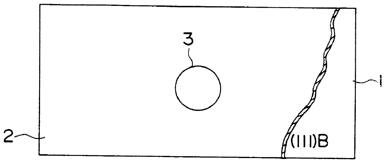
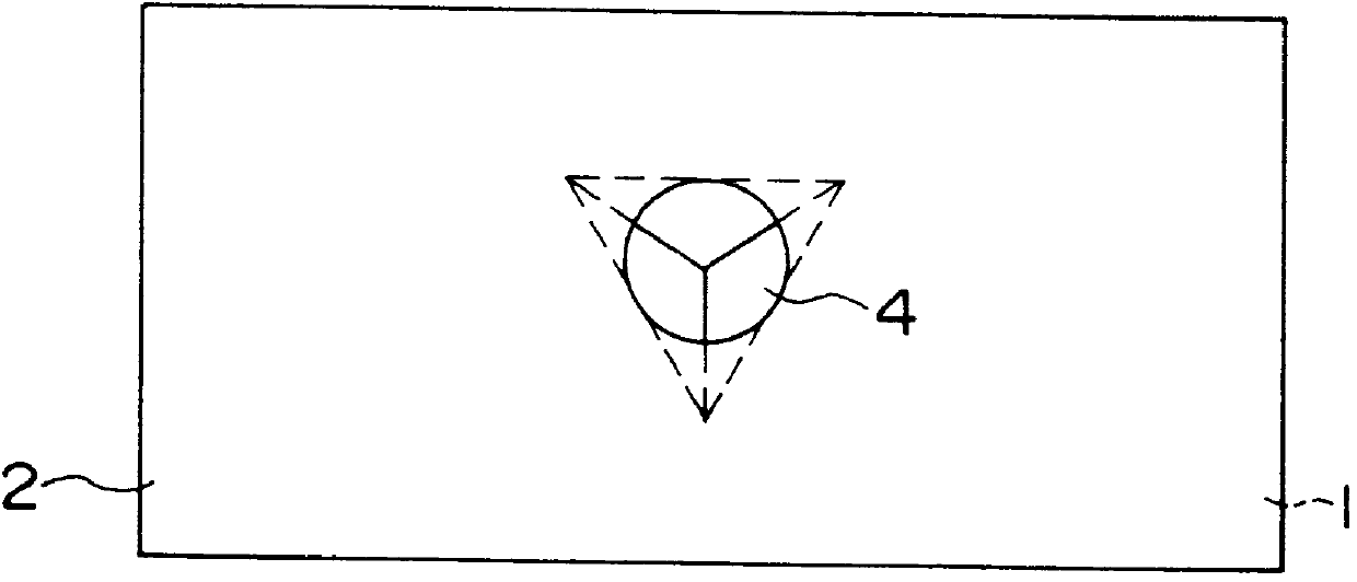
In this case, it should be noted that either the regular triangle shape or the circular shape, as described in the first embodiment, may be used as the etching mask opening section. In the case of the circular shape, the concave sections having the inverse regular triangular tetrahedron, which is formed to be circumscribed about the opening section, may be formed in an alignment manner.

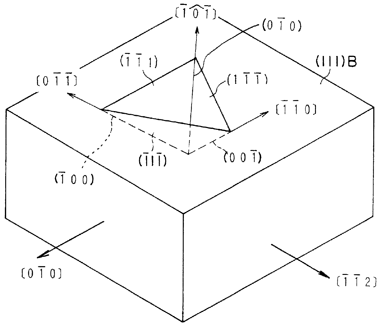
Next, as shown in FIG. 15D, by means of the reduced pressure MOVPE method using, as a growth preventing mask, the SiO.sub.2 film 53 used as the etching mask previously, an InAlAs barrier layer 56 of a thickness of 3 nm, an InGaAs well layer 57 of a thickness of 4 nm, and an InAlAs barrier layer 58 of a thickness of 3 nm are grown in the concave section so as to trace the shape of the concave section. Thereafter, an n type InGaAs emitter layer 59 and n.sup.+ type InGaAs contact layer 60 are grown so as to bury remaining section of the concave section.

In this case, if such growth conditions (i.e., growt...

second example

With reference to FIG. 17, a second example will be explained. FIG. 17 is a sectional view of a memory cell, corresponding to FIG. 15D. Only a structure of an emitter section of the second example will be explained because a structure formed from the substrate to the base layer is the same as in the first example including the face orientation.

An Fe-doped semi-insulating InP layer 52 grown on an n type InGaAs base layer 51 is processed by anisotropic etching using an SiO.sub.2 film 53 as the mask to thus form a concave section having an inverse regular triangular tetrahedron. After this, an i type InP barrier layer 66, an i type InGaAs well layer 57, and an i type InP barrier layer 67 are grown in the concave section so as to trace the shape of the concave section. Thereafter, an n type InGaAs emitter layer 59 and an n+type InGaAs contact layer 60 are grown so as to bury remaining section of the concave section.

In other words, in the second embodiment, the i type InAlAs barrier laye...

third example

With reference to FIG. 18, a third example will be explained. FIG. 18 is a sectional view of a memory cell, corresponding to FIG. 15D. Only a structure of an emitter section of the second example will be explained because a structure formed from the substrate to the base layer is the same as in the first example including the face orientation.

A p type or i type InP layer 68 is grown on an n type InGaAs base layer 51. Thereafter, the p type or i type InP layer 68 is processed by anisotropic etching using an SiO.sub.2 film 53 as the mask to thus form a concave section having an inverse regular triangular tetrahedron. After this, an i type InAlAs barrier layer 56, an i type InGaAs well layer 57, and an i type InAlAs barrier layer 58 are grown in the concave section so as to trace the shape of the concave section. Thereafter, an n type InGaAs emitter layer 59 and an n.sup.+ type InGaAs contact layer 60 are grown so as to bury remaining section of the concave section.

More particularly, i...


PUM


Abstract

In a semiconductor device, concave sections in which an opening area becomes small in proportion as a depth becomes deep are formed in a crystal layer, and a quantum structure is formed on at least one crystal face of a bottom section of the concave section and a border formed between plural sidewalls thereof. In case the quantum structure is formed in the bottom section, a quantum box is formed therein. If the quantum structure is formed in the border between the sidewalls of the concave section, a quantum wire is formed therein. In case the quantum structure is formed in the sidewall of the concave section, a two-dimensional quantum well is formed therein.

Description

2. Description of the Related ArtVarious fine patternings of semiconductor devices have been proposed, and semiconductor devices having new functions have also been proposed. Especially, a trend of forming various structures, which have not been achieved yet, on a semiconductor by employing crystal growth technology has been highly increased. In particular, a tendency of study has been raised such that new properties of matter, which are attained based on physical phenomena not found in the prior art, should be employed by forming a "quantum wire" or a "quantum box" so as to operate the semiconductor device. In the quantum wire or the quantum box, free carriers such as electrons and holes are confined in one or zero-dimensional potential energy by using a hetero junction structure of a compound semiconductor.If carriers are confined two-dimensionally, they move within one dimensional space (line). Such structure is called as the quantum wire. If carriers are confined three-dimension...

Claims


Application Information

Patent Timeline
IPC IPC(8): H01L21/306H01L21/02H01L21/20H01L29/02H01L29/12H01L29/04H01S5/227H01S5/00
CPCB82Y10/00H01L21/30612H01L29/045H01L29/125H01L29/127H01L21/02381H01L21/02543H01L21/02546H01L21/02642H01L21/0262H01S5/227
Inventor SAKUMA, YOSHIKISUGIYAMA, YOSHIHIROMUTO, SHUNICHI
Owner FUJITSU LTD
Why Eureka
Try Eureka