Adaptive addressable circuit redundancy method and apparatus

a technology of addressable circuits and redundancy methods, applied in the direction of information storage, static storage, digital storage, etc., can solve the problems of increased manufacturing costs of conventional methods, defective manufacturing of certain bits of memory, and difficulty in manufacturing such devices to have all words of memory operabl

Inactive Publication Date: 2000-01-04
AVAGO TECH WIRELESS IP SINGAPORE PTE +1
View PDF24 Cites 21 Cited by
  • Summary
  • Abstract
  • Description
  • Claims
  • Application Information

AI Technical Summary

Problems solved by technology

It is typically difficult to manufacture such devices to have all words of memory operable.
Oftentimes, certain bits of memory are defectively manufactured.
While being a well established method of memory ...

Method used


Image

  • Adaptive addressable circuit redundancy method and apparatus
  • Adaptive addressable circuit redundancy method and apparatus
  • Adaptive addressable circuit redundancy method and apparatus

Examples


Embodiment Construction

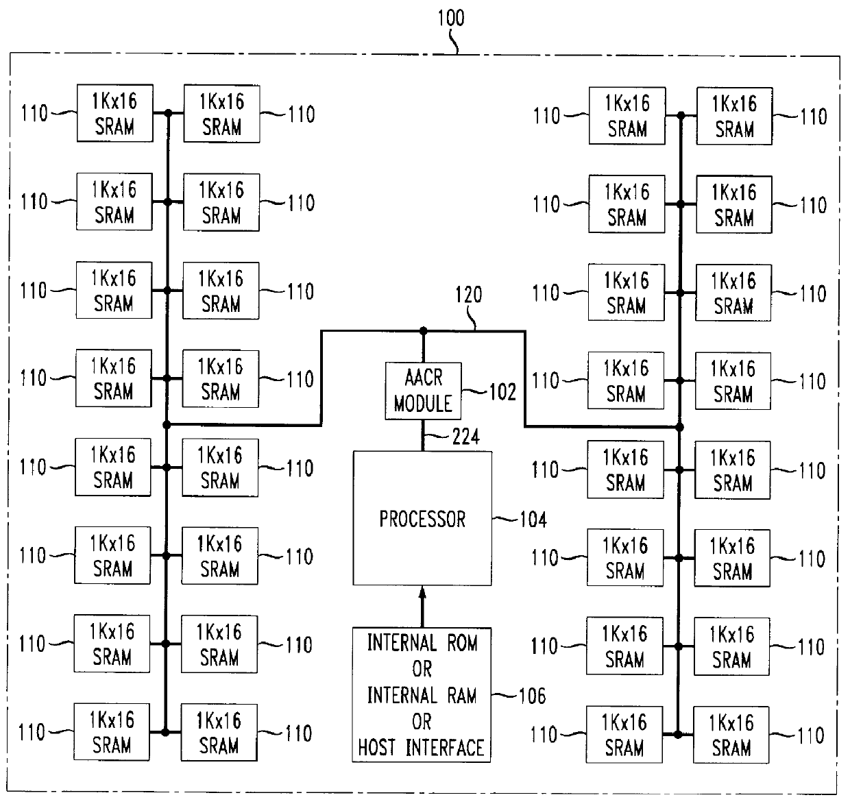
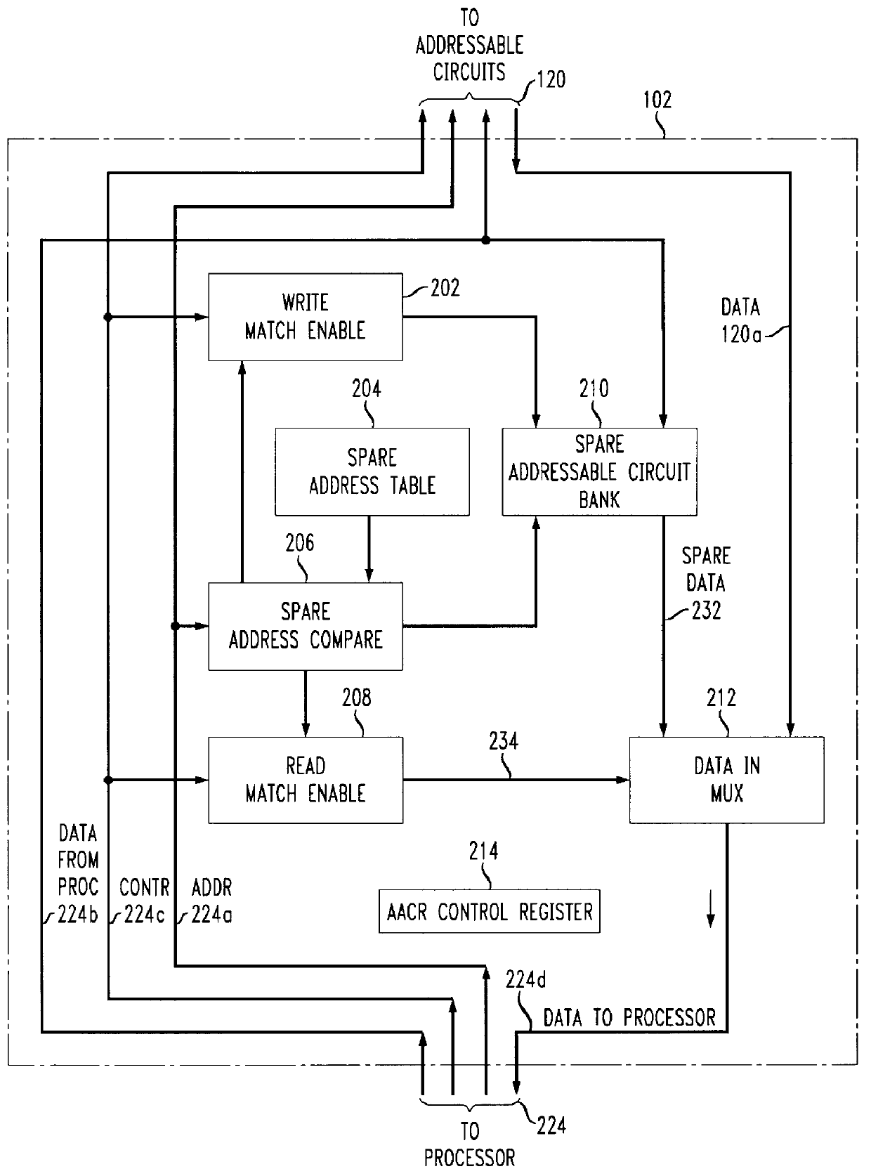
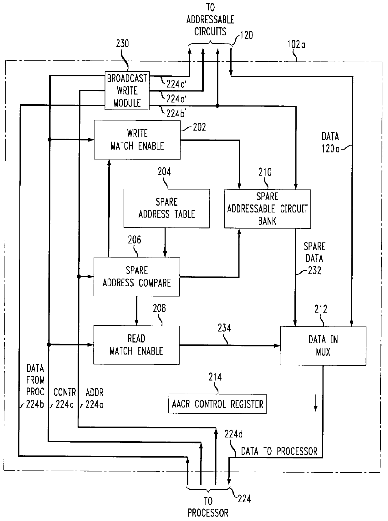
The present invention provides an improved redundancy method and apparatus which is particularly useful for large integrated circuits which include both an on-chip processor (e.g., a microprocessor, a microcontroller, or a digital signal processor (DSP)) and a significant amount of embedded addressable circuitry, e.g., random access memory (RAM) or read only memory (ROM).

While the present invention is described with respect to addressable embedded memory, the present invention is equally applicable to the replacement of any defective addressable circuitry which is made redundant to spare addressable circuitry.

The present embodiment of redundant memory presumes that a dominant memory failure mechanism is the failure of single bits or words of memory. This presumption is determined to be accurate based on an analysis of memory test / defect data. It is recognized by the present inventors that at least some of these single bit failures occur well after manufacture and packaging of the ...


PUM


Abstract

An adaptive addressable circuit redundancy method and apparatus, e.g., an adaptive memory redundancy method and apparatus, utilizes an on-chip processor to test, analyze and reassign spare addressable circuits to replace defective or intermittent addressable circuits. The present invention is applicable both in a manufacturing environment and/or in a field environment wherein the integrated circuit is operational. An adaptive addressable circuit redundancy module intercepts a data path between the on-chip processor and the addressable circuits to reassign defective addresses as necessary to utilize a spare addressable circuit bank. In another embodiment of the present invention, a broadcast write module cuts memory test time almost in half by writing a same data pattern to a significant portion or all of the addressable circuits, e.g., memory, substantially simultaneously.

Description

1. Field of the InventionThis invention relates to an adaptive memory redundancy method and apparatus for integrated circuits having an on-chip processor and embedded memory. More particularly, it relates to a method and apparatus to adaptively replace defective memory in a device including an on-chip processor and embedded memory.2. Background of Related ArtMany integrated circuits today include a processor and large amounts of embedded memory. It is typically difficult to manufacture such devices to have all words of memory operable. Oftentimes, certain bits of memory are defectively manufactured. However, instead of discarding the integrated circuit, memory redundancy techniques have been conventionally implemented which replace portions of the embedded memory containing defective bits so as to make the device acceptable for use. Thus, conventional memory redundancy techniques generally improve manufacturing yield.In conventional memory redundancy techniques, extra rows, columns ...

Claims


Application Information

Patent Timeline
IPC IPC(8): G11C29/00
CPCG11C29/70G11C29/72
Inventor FISCHER, FREDERICK HARRISONSINDALOVSKY, VLADIMIRSEGAN, SCOTT A.
Owner AVAGO TECH WIRELESS IP SINGAPORE PTE
Why Eureka
Try Eureka