Opto-electronic hybrid integration platform, optical sub-module, opto-electronic hybrid integration circuit, and process for fabricating platform

a technology of optoelectronic hybrid integration and fabrication platform, which is applied in the direction of optical elements, semiconductor lasers, instruments, etc., can solve the problems of not being able to achieve the circuit that satisfies the above three conditions, and the structure has a problem of considerably deteriorating the high-frequency characteristics of electrical wiring 6 and the resistance is not high enough to ensure high-frequency

Inactive Publication Date: 2000-02-22
NIPPON TELEGRAPH & TELEPHONE CORP
View PDF14 Cites 79 Cited by
  • Summary
  • Abstract
  • Description
  • Claims
  • Application Information

AI Technical Summary

Problems solved by technology

However, a circuit that satisfies the above three conditions has not been obtained with the prior art.
Further, the electrical wiring 6 is formed directly on the surface of the silicon substrate 1, or through a very thin oxide film of less than 0.5 .mu.m in thickness, but this structure has a problem of considerably deteriorating the high-frequency characteristics of the electrical wiring 6.
However, the silicon substrate 1 is very thin, the resistance is not high enough to ensure high-frequency characteristics, and it has a specific resistivity of about 1 k-ohm.cm.
Since, in such a structure, the core is only covered with very thin cladding layers 7b and 7c, it has problems that (1) the optical waveguide has a large loss, (2) it is liable to be affected by an external disturbance, and (3) formation of a directional coupler circuit is difficult.
In particular, the directional coupler is an indispensable circuit element to fabricate a high-performance optical circuit, and the impossibility of its formation means that application of the ridge type optical waveguide is limited to a narrow area.
Thus, the ridge type optical waveguide does not sufficiently satisfy the optical waveguide function.
Further, the electrical wiring function is not investigated here.
However, even with this circuit, the optical waveguide 13 is limited to the ridge type, tends to be affected by an external disturbance, and cannot provide a low loss optical waveguide function.
However, even with this circuit, the optical waveguide 18 is limited to the ridge type, tends to be affected by an external disturbance, and cannot provide a low loss optical waveguide function.
Therefore, it has a large transmission loss, tends to be affected by an external disturbance, and does not satisfy a sufficient optical waveguide function.
Further, in the above device, since the electrical wiring 28 is provided on the silicon substrate 1, the requirements for high-frequency characteristics are not satisfied.
As described above, the prior art hybrid optical integration technology does not satisfy the above three requirements.

Method used


Image

  • Opto-electronic hybrid integration platform, optical sub-module, opto-electronic hybrid integration circuit, and process for fabricating platform
  • Opto-electronic hybrid integration platform, optical sub-module, opto-electronic hybrid integration circuit, and process for fabricating platform
  • Opto-electronic hybrid integration platform, optical sub-module, opto-electronic hybrid integration circuit, and process for fabricating platform

Examples


embodiment 1

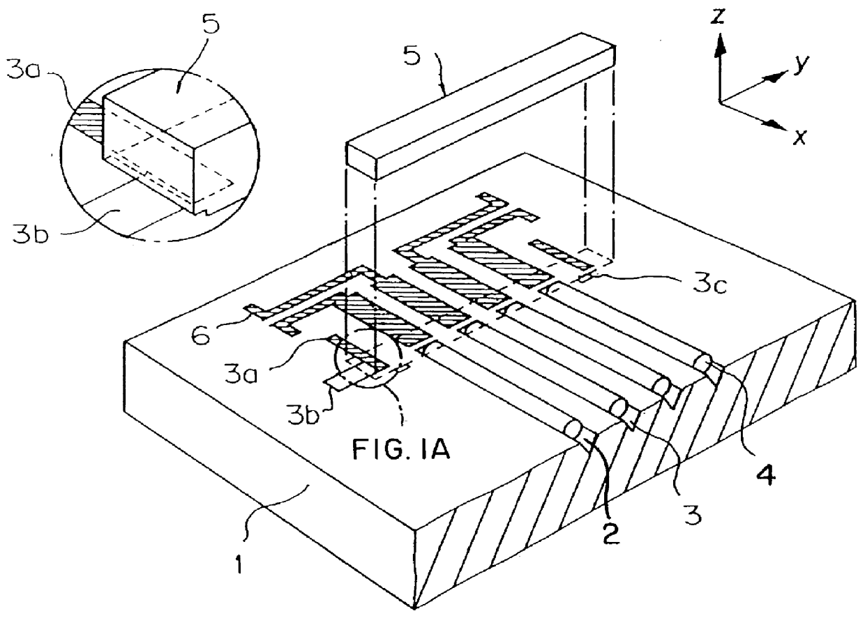
FIG. 9 is a schematic perspective view showing a first embodiment of the hybrid optical integrated circuit of the present invention. The reference numeral 1 indicates a substrate, and the present embodiment uses a silicon substrate provided with a protrusion and a recess on the surface. The reference numeral 30 indicates a silicon terrace which functions as an optical device mounting part, utilizing the protruded upper surface of the silicon substrate 1. The reference numeral 31 indicates an optical fiber used as an optical waveguide of the present embodiment, which is held in an optimum position in a V-groove provided in the silicon terrace 30. The reference numeral 52 indicates a thin film electrode for contacting with the surface electrode of an optical functional device 37 disposed on the silicon terrace 30, which is formed by patterning 1 .mu.m thick Au-Sn solder on a 0.5 .mu.m thermal oxide film provided on the silicon terrace 30 surface. This thin film electrode 52 is electri...

embodiment 2

FIG. 10 is a schematic perspective view showing the entire construction of a second embodiment of the optical / electronic hybrid optical integrated circuit of the present invention. FIG. 11 is a schematic cross sectional view in the vicinity of the circuit shown in FIG. 10, FIG. 12 is a cross-sectional view taken along surface 12--12 in FIG. 10, and FIG. 13 is a cross sectional view taken along surface 13--13 in FIG. 10.

As shown in FIG. 10, the packaged substrate of the present embodiment uses the silicon substrate 1 provided with a protrusion and a recess on the surface as in Embodiment 1. In the optical waveguide unit, a silica-based optical waveguide 40 is formed in the recess of the silicon substrate 1. As shown in FIG. 12, the silicon terrace 35 is provided on an electronic circuit mounting part. In the electrical wiring portion, a dielectric layer 50 comprising a polyimide resin is formed in the recess of the silicon substrate, the conductor patterns 51 and 510 are provided on ...

embodiment 3

FIG. 15 is a schematic perspective view showing the construction of a third embodiment of the hybrid optical integrated circuit of the present invention. A major difference of the present embodiment from Embodiment 2 is that the dielectric layer of the electrical wiring portion is formed using the same material as the optical waveguide.

That is, the silicon recess is formed by providing a 33 .mu.m step from the silicon terrace surface with the optical waveguide and the electrical wiring portion. In the silicon recess corresponding to the optical waveguide, the silica-based optical waveguide 40 having the under-clad 41 (35 .mu.m thick), the core 42 (6 .mu.m.times.6 .mu.m), and the over-clad 43 (30 .mu.m thick) is formed. On the other hand, on the silicon recess corresponding to the electrical wiring portion, the under-clad layer 41 of the silica-based optical waveguide is formed as the dielectric layer 50. It has a thickness of 25 .mu.m, and is 10 .mu.m lower than the upper surface of...


PUM


Abstract

An opto-electronic hybrid integrated circuit of the present invention satisfy a low-loss optical waveguide function, an optical bench function and a high-frequency electrical wiring function. The circuit includes a substrate such as a silicon substrate, a dielectric optical waveguide part arranged in a recess of the substrate, and an optical device mounting part formed on a protrusion of the substrate. An electrical wiring part is disposed on the dielectric layer. The optical device is mounted on the substrate. An optical sub-module includes the optical device which is possible to mount on the substrate.

Description

1. Field of the InventionThe present invention relates to a hybrid optical integration platform capable of incorporating an optical device or optical sub-module used for optical communication and optical signal processing in addition to optical waveguides and electrical wiring, an optical sub-module which can be equipped on an opto-electronic board, and a hybrid optical integrated circuit equipped with the optical device or optical sub-module, and to a process for fabricating the hybrid optical integration platform.2. Description of the Prior ArtWith recent advances in optical communication and optical information processing, development of an opto-electronic integration circuit is in demand. In such a circuit, active devices are incorporated in low-loss optical waveguides and the like to be driven by a high-frequency electrical circuit.To achieve a circuit incorporating active devices on the optical waveguide and driven at a high-frequency, three conditions are required for the opt...

Claims


Application Information

Patent Timeline
Patent Type & Authority Patents(United States)
IPC IPC(8): G02B6/42H01S5/20H01S5/02H01S5/062H01S5/00
CPCG02B6/42G02B6/4224G02B6/4227G02B6/4232G02B6/421G02B6/4219G02B6/4225G02B6/423G02B6/4238G02B6/4249H01S5/021H01S5/06226H01S5/2068H01L2224/45144H01L2924/00014H01L2224/48091H01L2924/19107H01L2924/3011H01L2924/00H01L2924/13055H01L2924/13091
Inventor YAMADA, YASUFUMIMINO, SHINJIOGAWA, IKUOTERUI, HIROSHIYOSHINO, KAORUKATO, KUNIHARUMORIWAKI, KAZUYUKISUGITA, AKIOYANAGISAWA, MASAHIROHASHIMOTO, TOSHIKAZU
Owner NIPPON TELEGRAPH & TELEPHONE CORP
Why Eureka
Try Eureka