

Layout method for a clock tree in a semiconductor device
a semiconductor device and clock tree technology, applied in the direction of generating/distributing signals, instruments, computer aided design, etc., can solve the problems of significant clock skew in the clock signal distribution circuit, difficult or substantially impossible to equalize the load of buffer drivers, and difficult or substantially impossible to equalize clock skew in the mesh clock circui
- Summary
- Abstract
- Description
- Claims
- Application Information
AI Technical Summary
Problems solved by technology
Method used
Image

Examples
Embodiment Construction
Now, the present invention is more specifically described with reference to accompanying drawings.
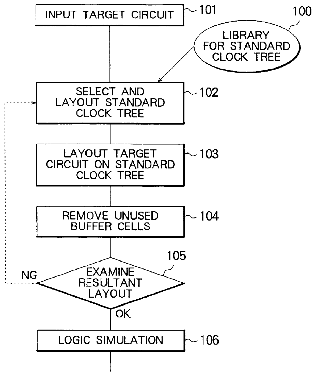
Referring to FIG. 1 showing a layout process for a clock signal distribution circuit according to an embodiment of the present invention, a layout system in a CAD system for designing the semiconductor integrated circuit to implement the layout process comprises a library 100 for storing data of standard clock trees, each of which defines a standard clock signal distribution circuit for a specific type of semiconductor integrated circuits or gate arrays. In each of the standard clock trees, a plurality of clock lines connecting a rout buffer and a plurality of buffer cells in a hierarchical format or a tree configuration have an equal line length. Before describing the steps of FIG. 1, the configuration of the standard clock trees will be described below.
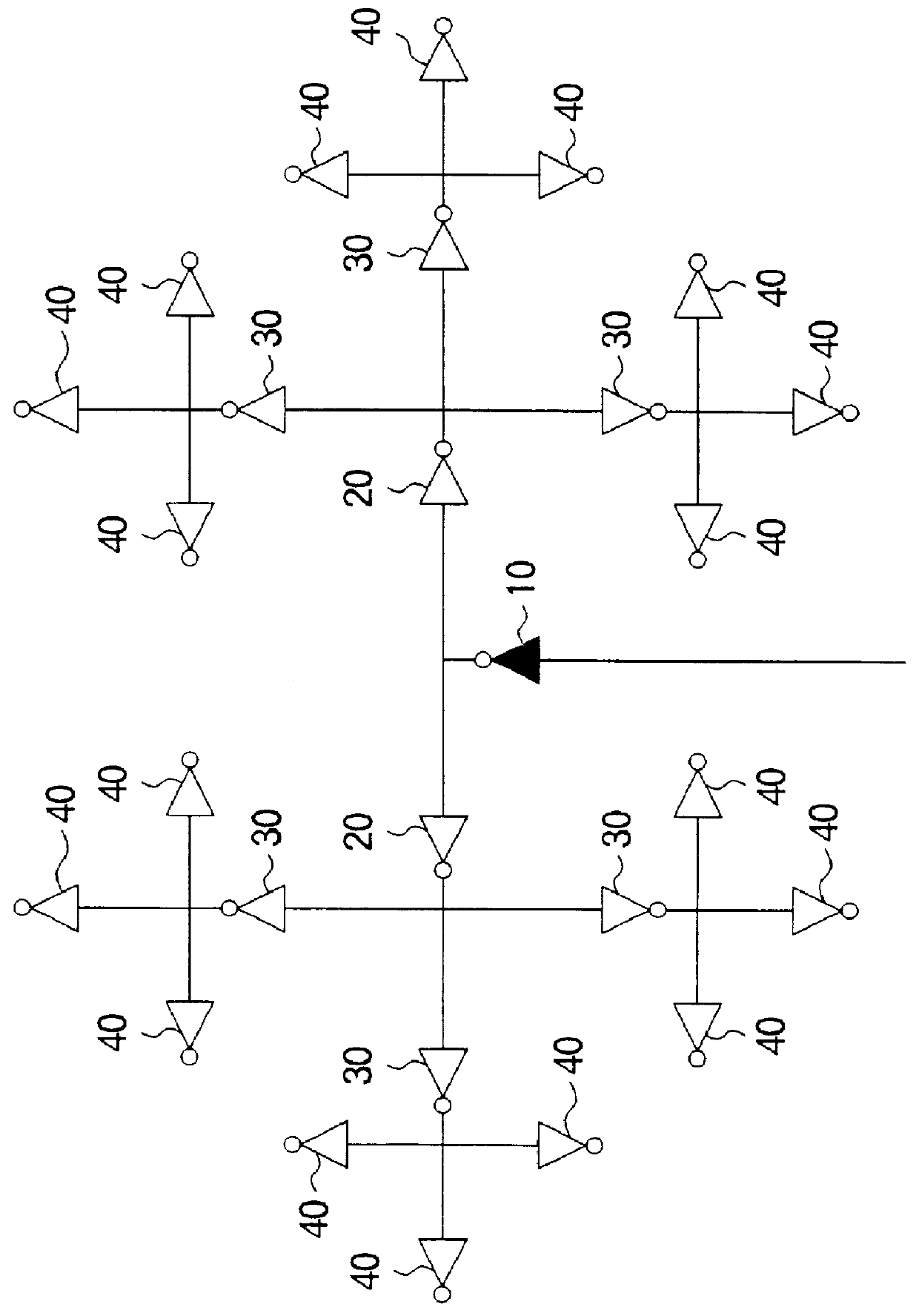
Referring to FIG. 2, there is shown an example of the standard clock trees stored in the library 100. The standard clock tree comprise...
PUM
 Abstract
Description
Claims
Application Information