

Solvent-assisted lithographic process using photosensitive sol-gel derived glass for depositing ridge waveguides on silicon
a sol-gel derived glass and solvent-assisted technology, applied in the direction of instruments, originals for photomechanical treatment, optics, etc., to achieve the effect of simple processing steps, no large capital investment in equipment, and rapid thermal annealing
- Summary
- Abstract
- Description
- Claims
- Application Information
AI Technical Summary
Benefits of technology
Problems solved by technology
Method used
Image

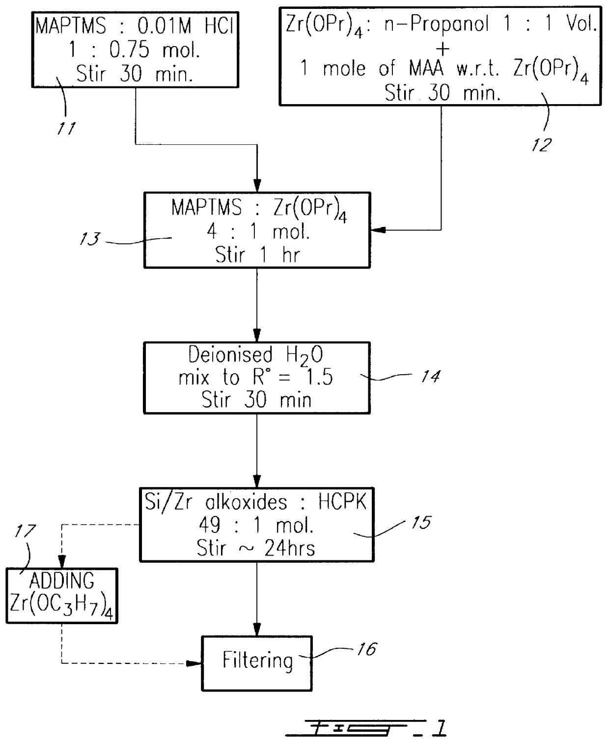
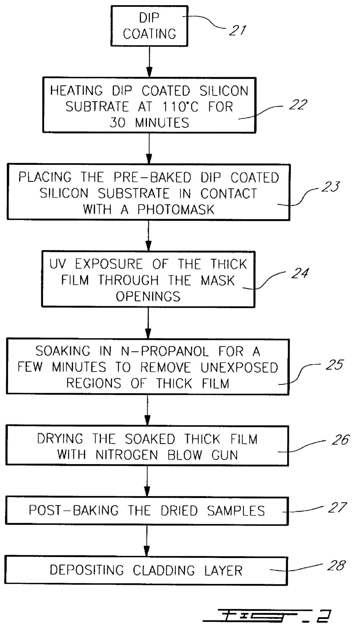
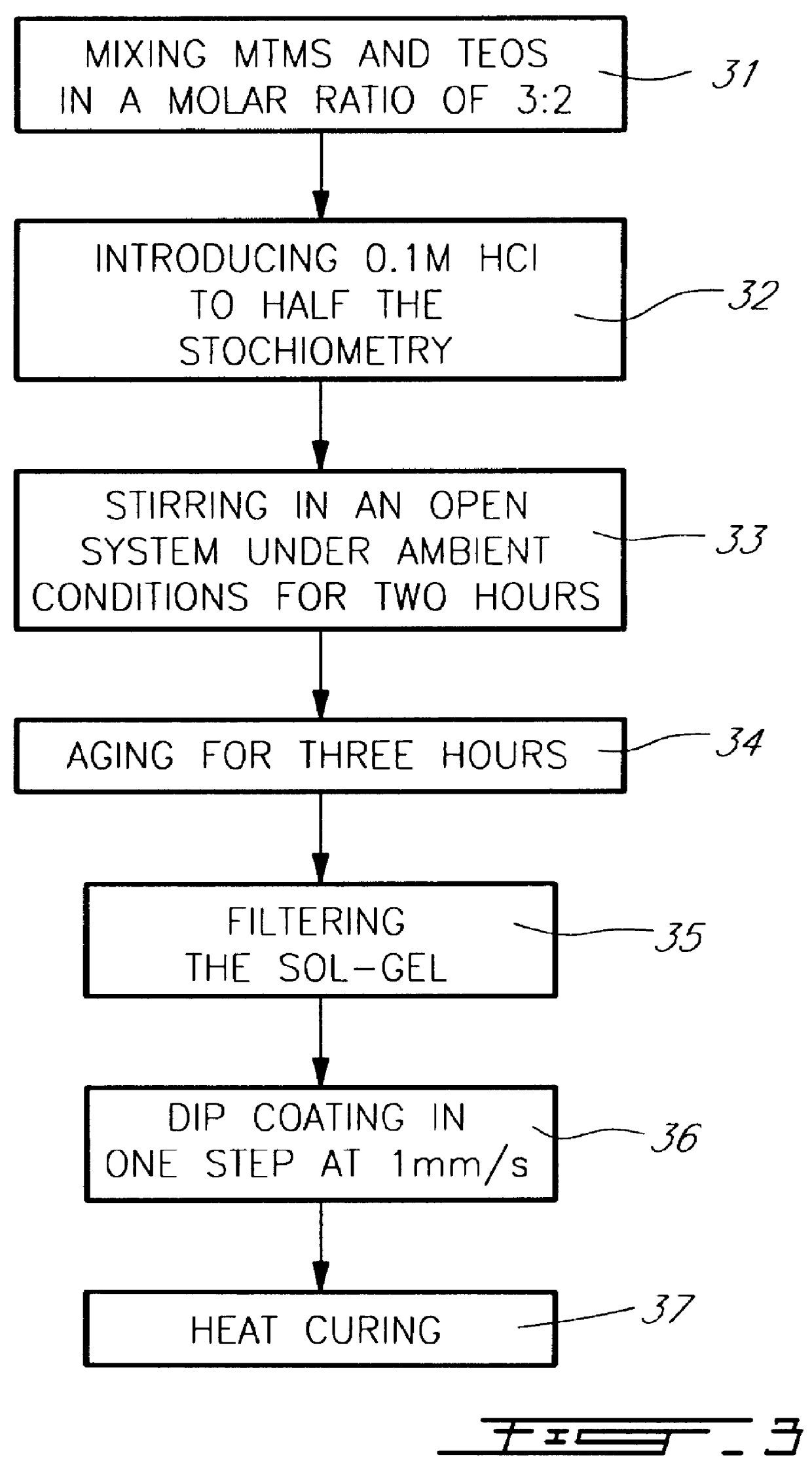
Examples
example 2
The ridge waveguide fabricating process according to the present invention can also be adapted to fabricate ridge waveguides with a sol-gel composition formulated by combining methacryloxypropyltrimethoxysilane (H.sub.2 C.dbd.C(CH.sub.3)CO.sub.2 (CH.sub.2).sub.3 Si(OCH.sub.3).sub.3), MAPTMS) and bis(s-butoxy)aluminoxytriethoxysilane specifically in the ratio 80 mole-percent methacryloxypropyltrimethoxysilane and 20 mole-percent bis(s-butoxy)aluminoxytriethoxysilane, using 1.5 equivalent of acidified (HCl) water (molar ratio of the mixture of methacryloxypropyltrimethoxysilane and bis(s-butoxy)aluminoxytriethoxysilane to acidified (HCl) water equal to 1.5).
The fabrication process according to the invention presents, amongst others, the following advantages over the other photoinscription techniques in photosensitive, organically modified glasses such as for example laser writing and ablation:
a) precise definition of boundaries in ridge waveguides;
b) simplification of geometrical and ...
PUM
| Property | Measurement | Unit |
|---|---|---|
| temperature | aaaaa | aaaaa |
| molar ratio | aaaaa | aaaaa |
| molar ratio | aaaaa | aaaaa |
Abstract
Description
Claims
Application Information