Method for providing fluorine barrier layer between conductor and insulator for degradation prevention

a technology of fluorine barrier layer and conductor, which is applied in the direction of semiconductor devices, semiconductor/solid-state device details, electrical devices, etc., can solve the problems of serious concern about degradation and high cost for the industry

Inactive Publication Date: 2000-05-23
IBM CORP
View PDF15 Cites 77 Cited by
  • Summary
  • Abstract
  • Description
  • Claims
  • Application Information

AI Technical Summary

Benefits of technology

It is another object of the present invention to provide corrosion resistance for aluminum lines in contact with oxide insulator lines containing fluorine.
The present invention is easily integrated into and compatible with multilevel metallization schemes that are so important in VSLI technology. In general, only one additional step, viz., the fluorine-free barrier layer formation itself, need be incorporated into the process. Moreover, since the present invention is a robust technique for preventing degradation in metal wiring lines and metallization interconnect features, considerable cost savings are achieved due to lowered failure rates and degradation monitoring requirements.

Problems solved by technology

This degradation is a serious concern because it represents a potential failure mechanism for an IC (integrated circuit).
The degradation problem is costly to the industry by virtue of the process monitoring, inspections, and equipment maintenance requirements that it entails.

Method used


Image

  • Method for providing fluorine barrier layer between conductor and insulator for degradation prevention
  • Method for providing fluorine barrier layer between conductor and insulator for degradation prevention
  • Method for providing fluorine barrier layer between conductor and insulator for degradation prevention

Examples


Embodiment Construction

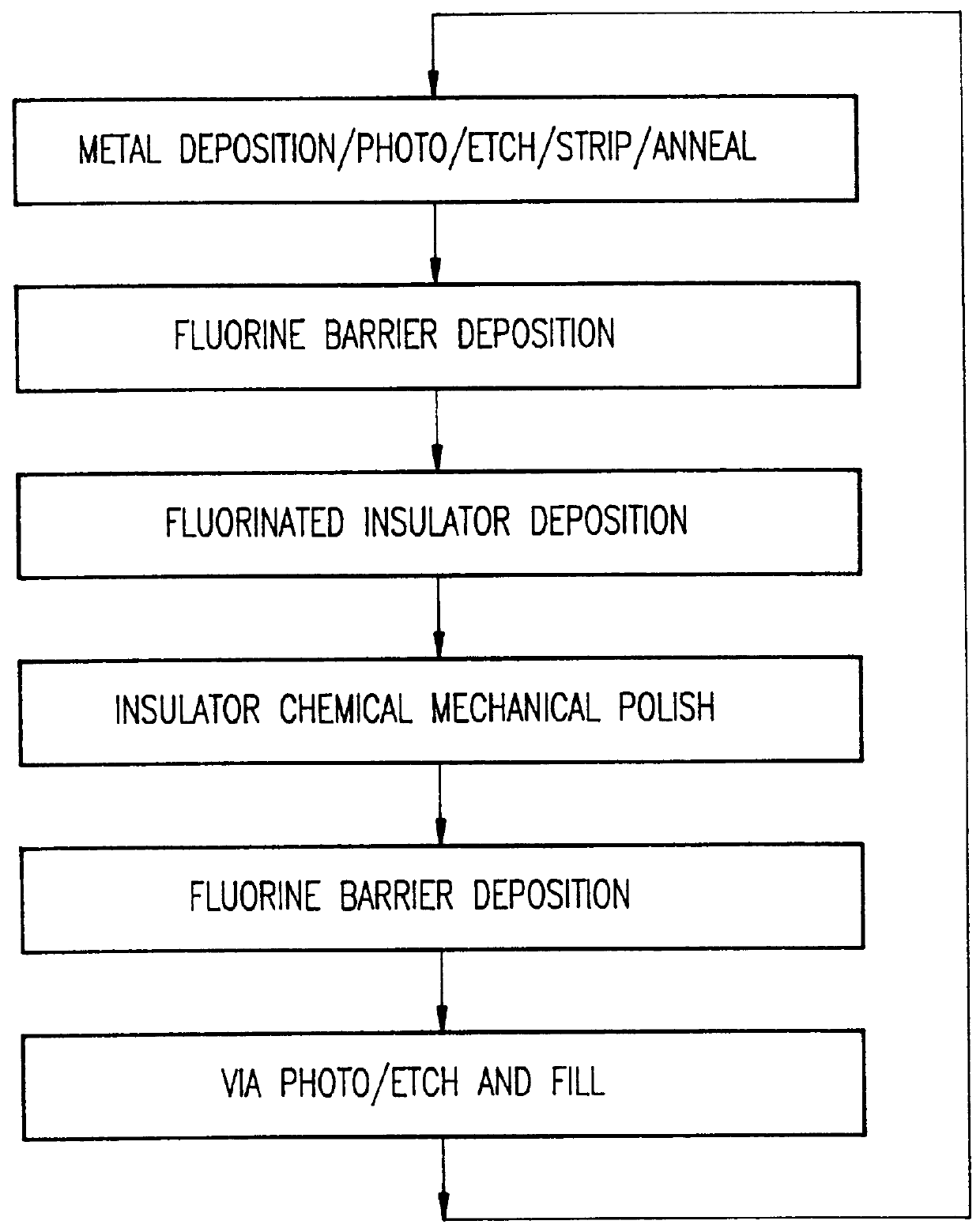
Referring now to the drawings, and more particularly to FIG. 1, there is shown a flow chart of one embodiment of the inventive method relating to additive formation of the fluorine-free barrier layer. The inventive processing sequence as summarized in FIG. 1 proceeds according to the following sequence of steps:

(a) metal wiring pattern formation by the sequentially executed substeps of metal deposition / photolithographic masking / etching / mask stripping / annealing;

(b) fluorine barrier deposition (lower layer);

(c) fluorinated insulator deposition;

(d) insulator chemical mechanical polish;

(e) fluorine barrier deposition (upper layer);

(f) contact formation by photolithographic masking / via formation by etching / via filling with metal and second level wiring formation; and

repeat steps (a)-(f) for any additional desired levels of metallization.

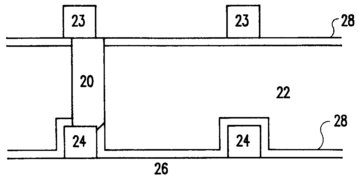
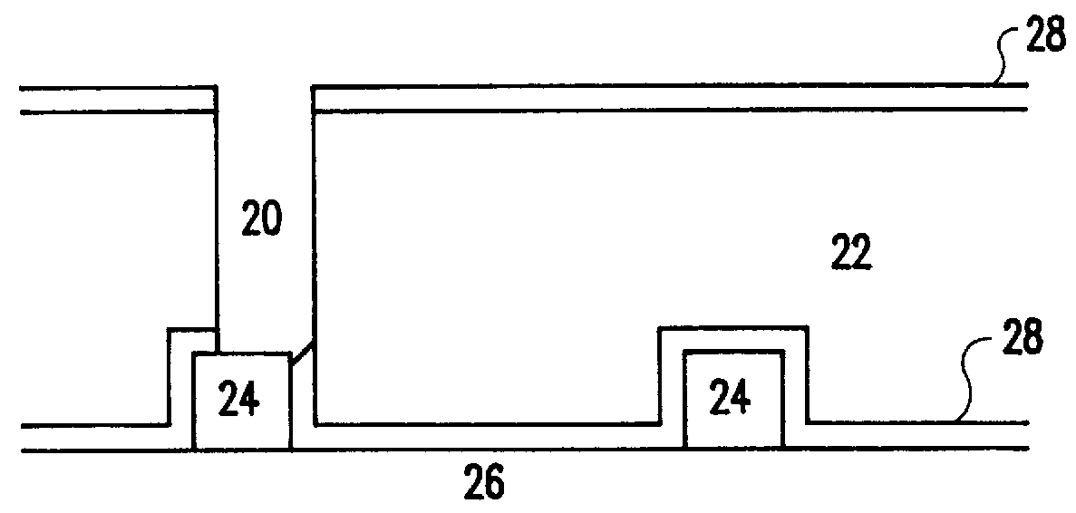
An implementation of this additive process is illustrated in FIGS. 2A-2F, respectively. In FIG. 2A, the formation of metal wiring pattern 24 is shown res...


PUM

PropertyMeasurementUnit
thicknessaaaaaaaaaa
thicknessaaaaaaaaaa
thicknessaaaaaaaaaa

Abstract

Method of improving the resistance of a metal against degradation from exposure to fluorine released from a fluorine-containing material by forming a fluorine-free silicon dioxide barrier layer between the insulator material and the metal. The invention is especially useful in improving corrosion and poisoning resistance of metallurgy, such as aluminum metallurgy, in semiconductor structures. The invention also covers integrated circuit structures made by this method.

Description

1. Field of the InventionThe present invention generally relates to semiconductor devices and manufacturing and, more particularly, to methods and structures which prevent degradation in semiconductor device wiring.2. Background DescriptionDegradation occurs in metal lines in contact with insulator materials containing fluorine. This degradation is a serious concern because it represents a potential failure mechanism for an IC (integrated circuit). The degradation problem is costly to the industry by virtue of the process monitoring, inspections, and equipment maintenance requirements that it entails. No understanding of, much less a solution to, the degradation problem associated with metal lines in contact with insulators containing fluorine has been developed prior to the present invention.It is therefore an object of the present invention to provide degradation resistance for metals in contact with fluorine-containing insulator materials.It is another object of the present inven...

Claims


Application Information

Patent Timeline
Patent Type & Authority Patents(United States)
IPC IPC(8): H01L21/02H01L21/285H01L21/768H01L21/70H01L21/314H01L21/316H01L23/522
CPCH01L21/28568H01L21/76801H01L21/76814H01L21/76826H01L21/76828H01L21/76831H01L21/76832H01L21/76834H01L21/76835H01L21/76838H01L21/76829Y10S438/963H01L21/31
Inventor COONEY, III, EDWARD C.LEE, HYUN K.MCDEVITT, THOMAS L.STAMPER, ANTHONY K.
Owner IBM CORP
Why Eureka
Try Eureka