Integrated laser imaging and spectral analysis system

a laser imaging and spectral analysis technology, applied in the field of optics, can solve the problems of inability to design the review station with little engineering, and the defect of the process flow is different between the actual and the undesired particle that sometimes becomes attached,

Inactive Publication Date: 2000-05-30
UNIPHASE A CA
View PDF2 Cites 107 Cited by
  • Summary
  • Abstract
  • Description
  • Claims
  • Application Information

AI Technical Summary

Problems solved by technology

Particulate defects are undesired particles that sometimes become attached to the surface of a wafer due to contamination in the wafer processing environment.
Process flow defects are differences between the actual and desired process result.
Little engineering was done in the design of these review stations.
The off-the-shelf microscopes currently being used in defect review stations lack sufficient resolution to resolve sub-micron defects.
However, the use of such microscopes increases the risk of contamination of the semiconductor chips during the review process, since a human is relatively dirty by cleanroom standards and is in close proximity to the wafer surface when using the microscope.
Furthermore, the presence of the microscope causes turbulent flow of the air near the wafer which tends to pull in nearby contaminants to the wafer.
Unfortunately, EDX analysis requires high voltage (up to approximately 40,000 volts) SEMS.
Furthermore, bombardment of the wafer surface with electrons from high voltage SEMs damages the wafer, thereby decreasing die yield.
Recently, low voltage SEMs (100-1000 volts) have seen limited use in wafer fabs for "critical dimension" measurements of line widths.
However, low voltage SEMs are too slow to use except on a sample basis, and, in addition, provide no analytical (e.g., EDX) capability.
Further, in both high and low voltage SEMs, the time to load samples into the SEM and pump down the load-lock chamber containing the SEM is relatively long, thereby slowing down wafer processing.
EDX technology also suffers in that only elemental information, not molecular structure information, is obtained about the bombarded surface.
However, no information is gleaned as to whether the surface is diamond, graphite, or carbon dust.
EDX technology also does not provide enough signal amplitude to analyze very light elements such as hydrogen.
EDX technology is also limited to particulates of over a micron or more in size unless the particulate is a high Z material.
However, such systems are relatively expensive, require a time consuming vacuum pump down, and still lack the ability to analyze molecular structures or sub-micron particles.
Thus, the resolution is too imprecise to detect sub-micron defects.

Method used


Image

  • Integrated laser imaging and spectral analysis system
  • Integrated laser imaging and spectral analysis system

Examples


Embodiment Construction

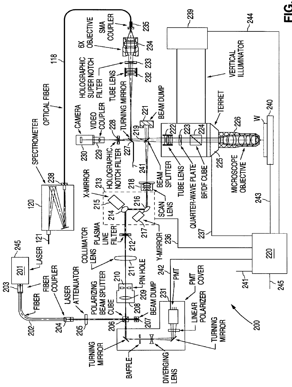
A dual mode integrated laser imaging and spectral analysis system according to the invention is used to view and analyze defects on a workpiece such as a semiconductor wafer. The system uses confocal laser scanning microscopy when operating in scanned imaging mode. Furthermore, defect spectral analysis uses a computer controlled spectrometer optically coupled to the confocal microscope when operating in stop scan spectral analysis mode.

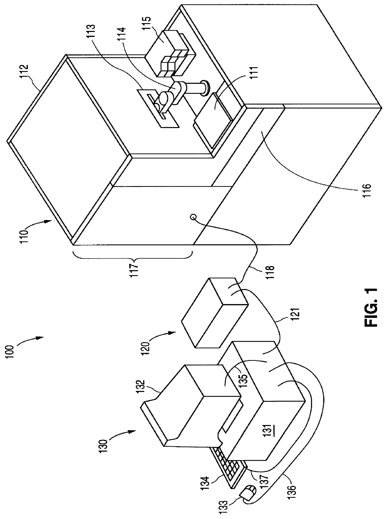
FIG. 1 is a perspective view of integrated laser imaging and analysis system 100 (hereinafter, "system 100") according to the invention. System 100 includes a main unit 110, a spectrometer 120 and a computer 130 which are interconnected. Main unit 110 performs confocal microscopy on a workpiece (e.g., a wafer) which is loaded into main unit 110 for analysis. Main unit 110 also includes a computer for controlling the confocal microscopy and for selectively providing light reflected by the wafer through an optical fiber to spectrometer 120. Spectrometer...


PUM

PropertyMeasurementUnit
diameteraaaaaaaaaa
diameteraaaaaaaaaa
diameteraaaaaaaaaa

Abstract

A system for analyzing an object has two operating modes such as scanned imaging mode and stop scan spectral analysis mode. A beam scanner is optically connected to a laser to receive laser beams from the laser. Beam scanner also scans the beams if the system is in the scanned imaging mode. A lens (e.g., an objective lens) is optically coupled to the beam scanner to focus the beams received from the beam scanner. A sensor is optically coupled to the lens to receive the beams that reflect from the object. The sensor may detect characteristics of the beam such as color and intensity. A spectrometer is optically coupled to the objective lens. During stop scan spectral analysis mode, spectrometer generates wavelength spectrum data.

Description

1. Field of the InventionThis invention relates to optics and, in particular, to an integrated laser imaging and spectral analysis system.2. Related ArtSemiconductor chip manufacturers have increasingly sought to improve die yields in their production processes even with ever decreasing minimum feature sizes ("die yield" is defined as the percentage of final working dies to total attempted dies). Key to this effort is the examination of the physical features (e.g., defects) of the semiconductor wafer.Defects are classified broadly as particulate or process flow defects. Particulate defects are undesired particles that sometimes become attached to the surface of a wafer due to contamination in the wafer processing environment. Process flow defects are differences between the actual and desired process result. The examination of particulate defects is important to determine the impact of such contamination on future process steps and ultimately on the functionality of the final die pa...

Claims


Application Information

Patent Timeline
Patent Type & Authority Patents(United States)
IPC IPC(8): G01J3/28
CPCG01J3/44G01J3/2823
Inventor XU, JAMES J.WORSTER, BRUCELEE, KEN K.
Owner UNIPHASE A CA
Why Eureka
Try Eureka