Methods for forming high-performing dual-damascene interconnect structures

a dual-damascene, interconnecting technology, applied in the direction of semiconductor devices, electrical equipment, semiconductor/solid-state device details, etc., can solve the problems of poor metal step coverage along the edges of contact openings, ineffective metal deposition and photolithographic techniques, and difficult control of wet chemical etch processes typically used with metals

Inactive Publication Date: 2000-06-06
NEWPORT FAB
View PDF5 Cites 254 Cited by
  • Summary
  • Abstract
  • Description
  • Claims
  • Application Information

AI Technical Summary

Problems solved by technology

However, the decreasing depth of focus that accompanies this increase in resolution requires the production of highly planar surfaces during intermediary process steps.
In light of the need for highly planar surfaces, traditional metal deposition and photolithographic techniques become progressively more ineffective as line widths are scaled down and multiple layers of metal are used.
For example, traditional metal deposition techniques can result in poor metal step coverage along the edges of the contact openings.
Furthermore, wet chemical etch processes typically used with metals are difficult to control.
While dry plasma etching may be employed with many metals, other metals with highly desirable properties (e.g., copper and gold) are generally not amenable to dry etching.
This localized pressure creates mechanical strain on the chemical bonds comprising the surface being polished, rendering the chemical bonds more susceptible to chemical attack by the slurry.
The use of Cu as interconnect metal in IC devices gives rise to many difficulties and challenges.
For example, as is well known, placing copper in contact with silicon or silicon dioxide can lead to disastrous results.
Specifically, copper tends to migrate or diffuse into the silicon dioxide, where it acts to increase leakage currents or actually short-out adjacent conductors.
In addition, once Cu diffuses through the silicon dioxide and reaches the silicon devices, the device will generally malfunction in some manner.
The top surface of a Cu conductor, however, is m

Method used


Image

  • Methods for forming high-performing dual-damascene interconnect structures
  • Methods for forming high-performing dual-damascene interconnect structures
  • Methods for forming high-performing dual-damascene interconnect structures

Examples


Embodiment Construction

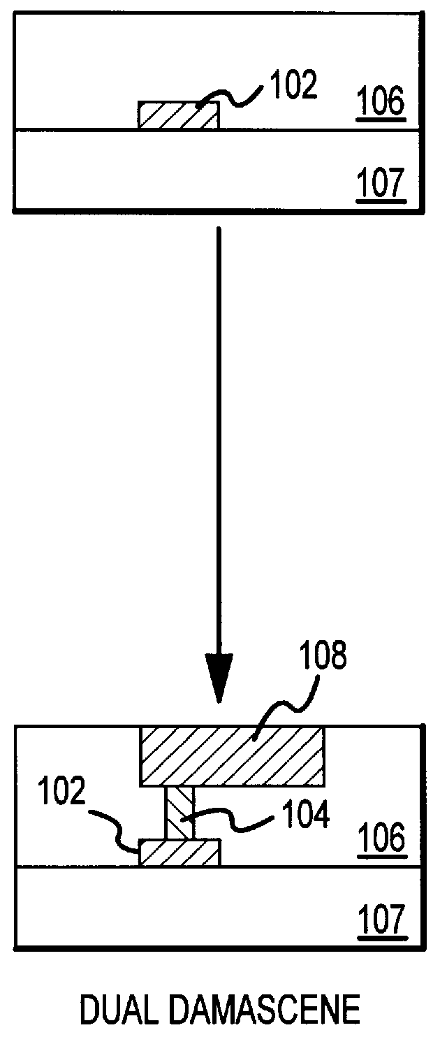
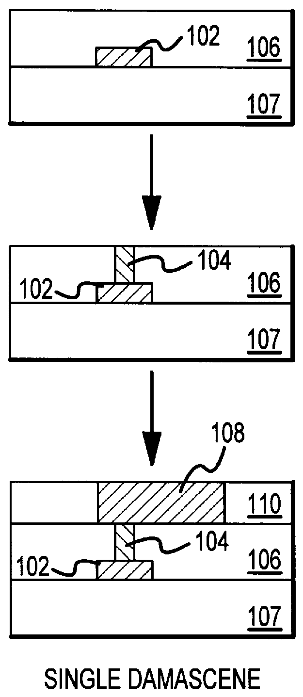
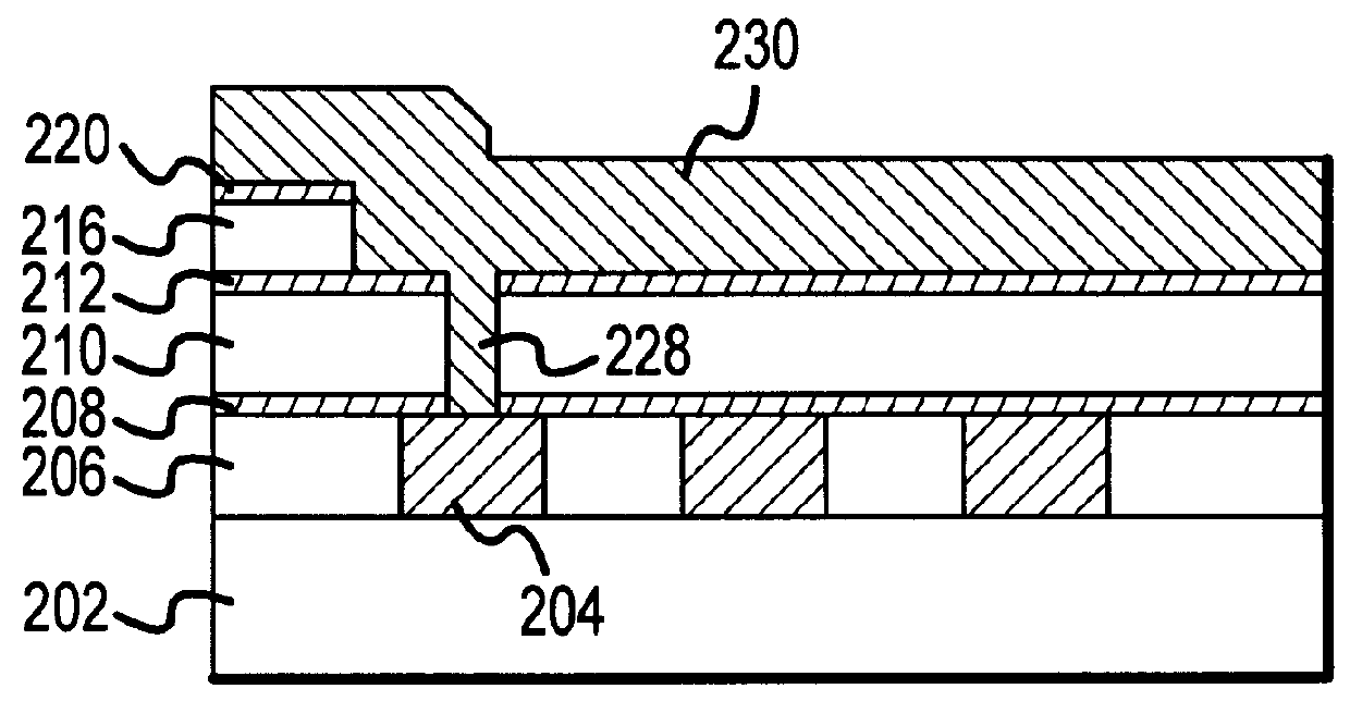
An interconnect fabrication process in accordance with various aspects of the present invention utilizes a dual-damascene approach with a CMP hard mask exhibiting excellent erosion resistance. Briefly, referring momentarily to FIG. 3J, a first hard mask layer 318 and a second hard mask layer 320 are employed. Hard mask layer 320, which protects hard mask layer 318 during various intermediate etch steps, is sacrificed during subsequent CMP processing. Thus, delamination of the low-k material is prevented, and any copper-contaminated material in hard mask layer 320 is removed.

More particularly, referring now to FIGS. 3 and 4, an exemplary dual damascene process in accordance with the present invention will now be described. In this regard, it should be understood that the illustrated process may include more or less steps or may be performed in the context of a larger processing scheme.

Initially, at Step 402, the first level metal (or, generally, a conductor) is obtained. That is, a f...


PUM


Abstract

Dual damascene methods and structures are provided for IC interconnects which use a dual-damascene process incorporating a low-k dielectric material, high conductivity metal, and an improved hard mask scheme. A pair of hard masks are employed: a silicon dioxide layer and a silicon nitride layer, wherein the silicon dioxide layer acts to protect the silicon nitride layer during dual damascene etch processing, but is subsequently sacrificed during CMP, allowing the silicon nitride layer to act as a the CMP hard mask. In this way, delamination of the low-k material is prevented, and any copper-contaminated silicon dioxide material is removed.

Description

The present invention relates, generally, to methods and structures for improving the fabrication of multilevel interconnects in integrated circuits and, more particularly, to a dual damascene, low-k dielectric process employing an improved hard-mask scheme.BACKGROUND ART AND TECHNICAL PROBLEMSThrough advanced semiconductor processing techniques, integrated circuit devices with submicron and sub-half-micron features sizes can now be manufactured. This trend toward deep submicron technology (i.e., involving feature sizes less than 0.35 microns) has, in turn, driven the need for multilayer interconnects. As a result, circuit performance in the deep submicron regime is increasingly a function of the delay time of electronic signals traveling between the millions of gates and transistors present on the typical integrated circuit chip. Parasitic capacitance and resistance effects resulting from these otherwise passive interconnect structures must therefore be well-controlled. Toward this...

Claims


Application Information

Patent Timeline
IPC IPC(8): H01L21/768H01L23/522H01L21/70H01L23/52H01L23/532
CPCH01L21/7681H01L21/76819H01L23/5329H01L23/5222H01L21/7684H01L2924/0002H01L2924/00
Inventor ZHAO, BIN
Owner NEWPORT FAB
Why Eureka
Try Eureka