Method of etching patterned layers useful as masking during subsequent etching or for damascene structures

a technology of patterned layers and damasks, applied in the field of etching of patterned layers, can solve the problems of film oxidization or other corrosion, distortion of pattern, removal of residual silicon dioxide hard masking material,

Inactive Publication Date: 2000-06-27
APPLIED MATERIALS INC
View PDF49 Cites 558 Cited by
  • Summary
  • Abstract
  • Description
  • Claims
  • Application Information

AI Technical Summary

Problems solved by technology

This could lead to distortion of the pattern which is transferred to conductive layer 106.
At this point, the problem is the removal of the residual silicon dioxide hard masking material and the removal of residue deposits of the silicon dioxide masking material from adjacent surfaces.
When a patterning mask for etch of a copper film is prepared, should these etchant species contact the copper film, the film is oxidized or otherwise corroded.
In addition, etchant species which contain oxygen, fluorine, chlorine or bromine leave deposits of etch byproduct on etched contact via and damascene structure surfaces which may cause oxidation and corrosion of copper depositions made over su...

Method used


Image

  • Method of etching patterned layers useful as masking during subsequent etching or for damascene structures
  • Method of etching patterned layers useful as masking during subsequent etching or for damascene structures
  • Method of etching patterned layers useful as masking during subsequent etching or for damascene structures

Examples


second embodiment

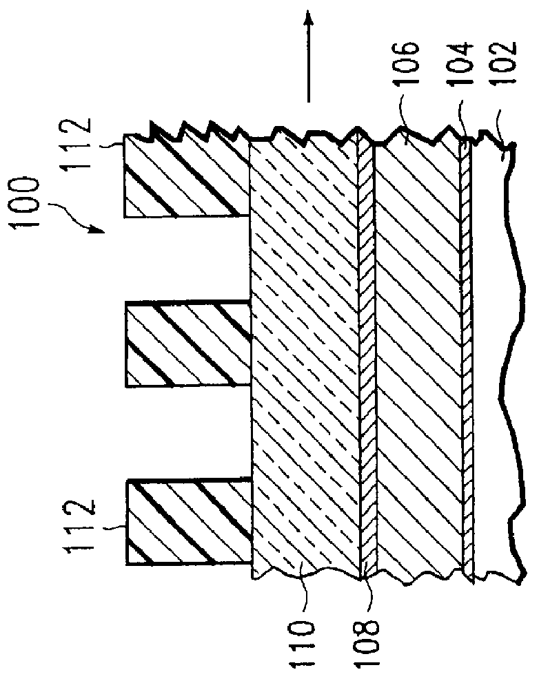
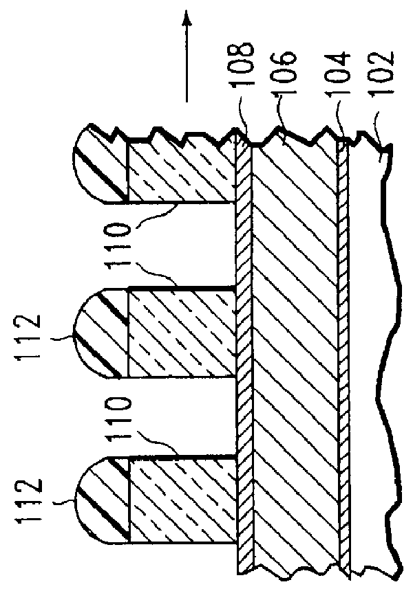
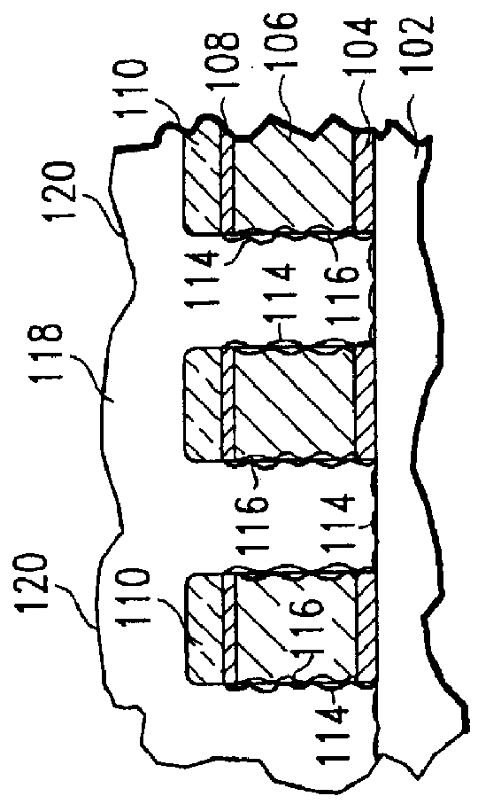
the present invention pertains to a specialized etch chemistry useful in patterning silicon-free organic polymeric layers such as low k dielectrics and other organic interfacial layers. This etch chemistry is particularly useful when the conductive material in a multilayered etch stack is copper, or when copper is the conductive fill material used for formation of a contact via, or in a damascene or dual damascene process.

By way of explanation, in a damascene process, the process steps would typically include: blanket deposition of a dielectric material; patterning of the dielectric material to form openings; deposition of a diffusion barrier layer and, optionally, a wetting layer to line the openings; deposition of a conductive layer such as copper, tungsten, or aluminum onto the substrate in sufficient thickness to fill the openings; and removal of excessive conductive material from the substrate surface using chemical-mechanical polishing (CMP) techniques or etch-back techniques....


PUM


Abstract

A first embodiment of the present invention pertains to a method of patterning a semiconductor device conductive feature while permitting easy removal of any residual masking layer which remains after completion of the etching process. A multi-layered masking structure is used which includes a layer of high-temperature organic-based masking material overlaid by either a patterned layer of inorganic masking material or by a layer of patterned high-temperature imageable organic masking material. The inorganic masking material is used to transfer a pattern to the high-temperature organic-based masking material and is then removed. The high-temperature organic-based masking material is used to transfer the pattern and then may be removed if desired. This method is also useful in the pattern etching of aluminum, even though aluminum can be etched at lower temperatures. A second embodiment of the present invention pertains to a specialized etch chemistry useful in the patterning of organic polymeric layers such as low k dielectrics, or other organic polymeric interfacial layers. This etch chemistry is useful for mask opening during the etch of a conductive layer or is useful in etching damascene structures where a metal fill layer is applied over the surface of a patterned organic-based dielectric layer. The etch chemistry provides for the use of etchant plasma species which minimize oxygen, fluorine, chlorine, and bromine content.

Description

1. Field of the InventionThe present invention pertains to a method for etching of patterned layers. The method is useful in high temperature etch processes where the layers are high temperature masking materials or are metal-comprising layers such as copper, platinum, iridium, and barium strontium titanate. The method is also useful in lower temperature etch processes in which organic polymeric layers, such as low k dielectrics, are etched to form damascene process structures. The present method may also be used for lower temperature etching of metal layers such as aluminum or tungsten, when the pattern geometry is small (less than about 0.25 .mu.m) and etch selectivity is a problem.2. Brief Description of the Background ArtIn the field of semiconductor device fabrication, particularly with the continuing trend toward smaller device feature sizes, the etch processes which are used to construct conductive features such a metal interconnects and contacts have become particularly crit...

Claims


Application Information

Patent Timeline
IPC IPC(8): H01L21/027H01L21/02H01L21/3213H01L21/311H01L21/312H01L21/316H01L21/314H01L21/302
CPCH01L21/0274H01L21/31138H01L21/31144H01L21/32139H01L21/31116H01L21/3146H01L21/31612H01L21/32136H01L21/3127H01L21/0212H01L21/02115H01L21/02164H01L21/306
Inventor YE, YANIONOV, PAVELZHAO, ALLENHSIEH, PETER CHANG-LINMA, DIANA XIAOBINGYAN, CHUNYUAN, JIE
Owner APPLIED MATERIALS INC
Why Eureka
Try Eureka