Method of making an interconnect using a tungsten hard mask

a technology of tungsten and hard mask, which is applied in the direction of semiconductor/solid-state device manufacturing, basic electric elements, electric apparatus, etc., can solve the problems of poor selectivity between metal and photoresist, process limitations are further compounded, and current lithographic processes are approaching the limits of the ability to resolve minimum features

Inactive Publication Date: 2000-07-11
ADVANCED MICRO DEVICES INC
View PDF7 Cites 228 Cited by
  • Summary
  • Abstract
  • Description
  • Claims
  • Application Information

AI Technical Summary

Benefits of technology

Use of the two step etch process exploits the etch selectivity difference between tungsten and aluminum and allows tungsten to advantageously operate as a hard mask, while reducing the thickness of the photoresist layer to provide improved metal pitch between metal layers.

Problems solved by technology

Current lithographic processes are approaching the limits of the ability of to resolve minimum features that are adequate for a manufacturing process.
The process limitations are further compounded by poor selectivity between metal and photoresist during a typical metal etch process.
As a result, thicker photoresist tends to limit the resolution.
However, as resists become thicker, it becomes harder to resolve smaller features with an acceptable depth of focus.
Unfortunately, at this thickness, the resolution of the photoresist may produce significant deviations between the desired pattern and the actual pattern transferred to the substrate.

Method used


Image

  • Method of making an interconnect using a tungsten hard mask
  • Method of making an interconnect using a tungsten hard mask
  • Method of making an interconnect using a tungsten hard mask

Examples


Embodiment Construction

)

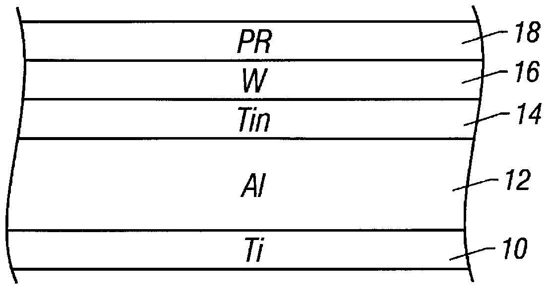
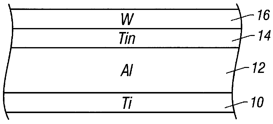
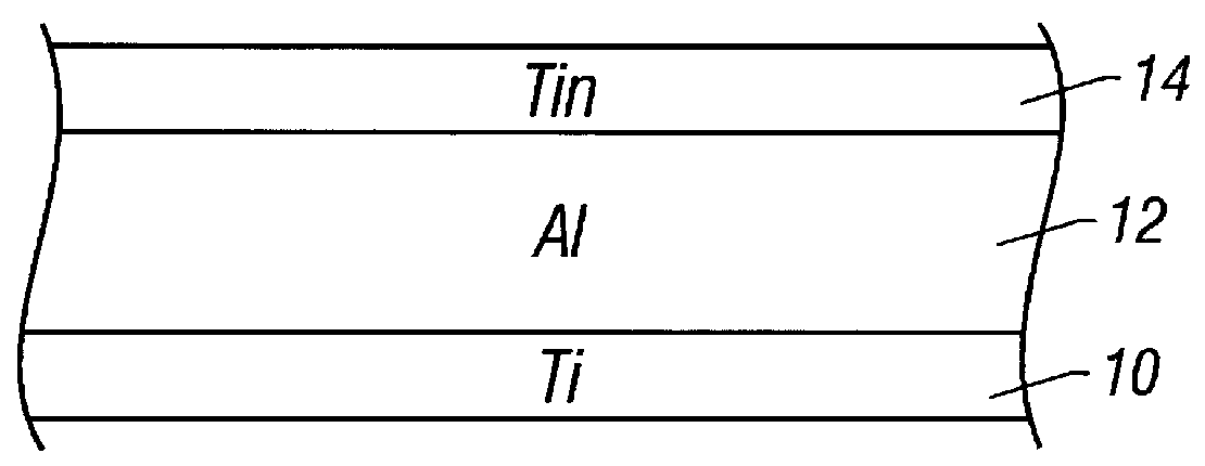
Referring to FIGS. 1 through 6, cross sectional views are shown illustrating the process steps in accordance with the present invention to form a metal interconnect. In the illustrated embodiment, as shown in FIG. 1, an aluminum based layer 12 of approximately 2 microns is formed over substrate 10 which may be a 250 angstrom titanium based layer. Layer 10 may be either titanium (Ti), titanium nitride (TiN) or both. Aluminum based layer 12 may be aluminum or an aluminum alloy doped with such materials as copper. The aluminum based layer 12 is deposited on titanium based layer 10 by sputtering or evaporation.

Then a titanium based layer 14 is deposited on aluminum layer 12 using sputtering or evaporation. Layer 14, which serves as an adhesion layer, may be a graded Ti / TiN layer in which approximately the first 150 angstroms is Ti and the next 200 angstroms are TiN. In the illustrated embodiment the Ti / TiN layer 14 has a thickness of approximately 350 angstroms but may range from 150 t...


PUM

PropertyMeasurementUnit
thicknessaaaaaaaaaa
thicknessaaaaaaaaaa
thicknessaaaaaaaaaa

Abstract

An interconnect layer is fabricated using a tungsten hard mask by forming a tungsten based layer over an aluminum based layer. A photoresist layer is deposited over the tungsten based layer and patterned. The tungsten based layer is patterned by applying a fluorine-based etchant using the photoresist layer as an etch mask. Then the aluminum based layer is patterned by applying a chlorine based etchant using the tungsten based layer as an etch mask.

Description

1. Field of the InventionThis invention relates to integrated circuit manufacturing and more particularly, to forming an interconnect using tungsten as a hard mask.2. Description of the Related ArtCurrent integrated circuit manufacturing processes typically use multiple levels of some form of metal interconnect to provide interconnections between various circuits on the integrated circuit. For instance, current manufacturing processes are known to use five levels of metal interconnects. The etch process to form the interconnect requires that precisely defined regions of metal be exposed to etchants in order to selectively remove material from those regions. The patterns that define the regions are typically created using lithographic processes. For instance, a layer of photoresist is spin-coated onto a substrate, and the resist layer is selectively exposed to a form of radiation, such as ultraviolet light, electrons, or x-rays.An exposure tool and mask, or data tape in electron beam...

Claims


Application Information

Patent Timeline
Patent Type & Authority Patents(United States)
IPC IPC(8): H01L21/02H01L21/3213H01L21/033H01L21/768H01L21/70
CPCH01L21/32139H01L21/0332H01L21/32136H01L21/76838
Inventor WILLIAMS, JOHN DAVID
Owner ADVANCED MICRO DEVICES INC
Why Eureka
Try Eureka