Process for integrated circuit wiring

a technology of integrated circuits and wiring, which is applied in the direction of resistive material coating, solid-state devices, metallic material coating processes, etc., can solve the problems of reducing yield, reducing yield, and reducing the effect of damascene process

Inactive Publication Date: 2000-09-12
IBM CORP
View PDF16 Cites 111 Cited by
  • Summary
  • Abstract
  • Description
  • Claims
  • Application Information

AI Technical Summary

Benefits of technology

An object of this invention is to provide a process that permits the preferential removal of a plating base or seed layer without significantly etching or distorting the plated features of interest. Moreover, an object of the present invention is to provide a process in which the desired seed layer features are defined prior to the metal deposition.

Problems solved by technology

Also, insulator gap fill and planarization may be more problematic.
Accordingly, the use of a damascene process may not provide a significant advantage for the last wiring level because of low thruput of the CMP step.
Also, erosion of the insulator adjacent to large metal feature is a source of yield loss, especially when they occur at lower levels.
However, the most difficult aspect of the thru-mask process is the seed layer etching step.
The loss of 100 nm in a 700 nm interconnection structure is a detrimental ground rule violation (see FIG. 2).

Method used


Image

  • Process for integrated circuit wiring
  • Process for integrated circuit wiring
  • Process for integrated circuit wiring

Examples


example

Alkanol ACN is dissolved in deionized water (DI) to make 2000 ppm by volume stock solution. Stirring is carried out for about 30 minutes to dissolve the Alkanol ACN in DI. A 5 g / l ammonium persulfate by wt. solution in DI is prepared and then acidified with sulfuric acid to pH 4. The Alkanol ACN stock solution is added to the acidified ammonium persulfate solution in an amount to provide 250 ppm by volume of the Alkanol ACN. The solution is stirred for about 20 minutes before use.

The resist is stripped from a plated substrate in a suitable solution for the resist. Next, the substrate is rinsed copiously with a DI cold water spray. The substrate is then immersed in a tank with the above Alkanol ACN / persulfate etchant solution with mild agitation. Etching is carried out about 5 minutes. The substrate is then rinsed vigorously in deionized water.

When the Alkanol ACN concentration is increased to about 500 ppm, the etch rate of copper in the ammonium persulfate solution is decreased.


PUM

PropertyMeasurementUnit
temperatureaaaaaaaaaa
thickaaaaaaaaaa

Abstract

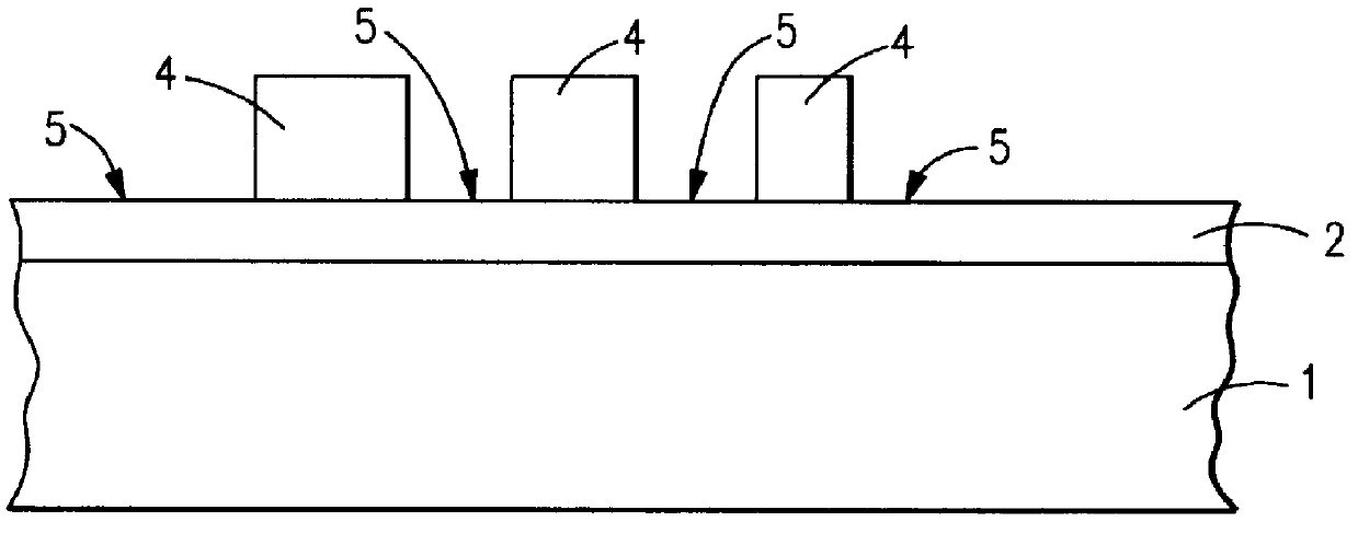
Metal wiring is provided in an integrated circuit by sputter coating onto a semiconductor substrate a copper seed layer; depositing and patterning a photoresist; electroplating or electrolessly plating a metal within the openings of the photoresist; stripping the remaining photoresist; and etching the copper seed layer with an etchant that preferentially etches the copper seed layer at a rate higher than that for the electroplated or electrolessly plated metal.

Description

The present invention is concerned with a process for fabricating metal wires in an integrated circuit. More particularly, the present invention is concerned with fabrication of copper wiring for chip interconnections and chip packaging. The methods of this invention use a thru-mask process instead of the damascene type technique to avoid problems of dishing in large metal features and erosion of insulators adjacent to comparatively large metal features.BACKGROUND OF INVENTIONVarious techniques have been investigated and used for metallizing semiconductor chips. These methods include the lift-off process, thru-mask methods, metal RIE and metal and insulator damascene and various combinations of the above methods. The lift-off and thru-mask methods are more valuable for large features like those typically encountered in chip packaging. Unlike the lift-off and the thru-mask methods, the metal RIE and damascene methods have been the process of choice for chip metallizations where the g...

Claims


Application Information

Patent Timeline
Patent Type & Authority Patents(United States)
IPC IPC(8): H01L21/02H01L21/768H01L21/70H01L21/285H01L21/288H05K3/10C23C18/31H01L21/302H01L21/3065H01L21/3205H05K3/06
CPCH01L21/2855H01L21/288H01L21/2885H01L21/76885H05K3/108H05K3/067H05K2201/0317H01L2924/0002H01L2924/00H01L21/768
Inventor UZOH, CYPRIAN EMEKA
Owner IBM CORP
Why Eureka
Try Eureka