Short-wavelength optoelectronic device including field emission device and optical device and its fabricating method

a short-wavelength optoelectronic and field emission technology, applied in the manufacture of electric discharge tubes/lamps, semiconductor lasers, electromechanical systems, etc., can solve the problems of inapplicability of ultra-violet lasers employing he--cd gas plasma or frequency modulation methods to microelectronics, difficult to fabricate optoelectronic devices using semiconductors, and large volume and high cos

Inactive Publication Date: 2000-10-31
ELECTRONICS & TELECOMM RES INST
View PDF5 Cites 65 Cited by
  • Summary
  • Abstract
  • Description
  • Claims
  • Application Information

AI Technical Summary

Problems solved by technology

However, ultraviolet lasers employing He--Cd gas plasma or frequency modulation method are inapplicable to the microelectronics because they are extremely large in volume and very expensive.
However, it is still difficult to fabricate an optoelectronic device using a semiconductor which operates in a short-wavelength band below 400 nm, and notably, there has never bee

Method used


Image

  • Short-wavelength optoelectronic device including field emission device and optical device and its fabricating method
  • Short-wavelength optoelectronic device including field emission device and optical device and its fabricating method
  • Short-wavelength optoelectronic device including field emission device and optical device and its fabricating method

Examples


Embodiment Construction

Hereinafter, the present invention will be described in detail with reference to the attached drawings.

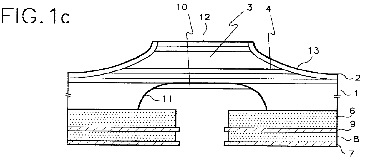
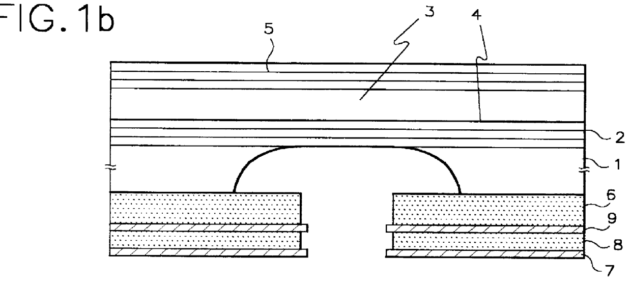
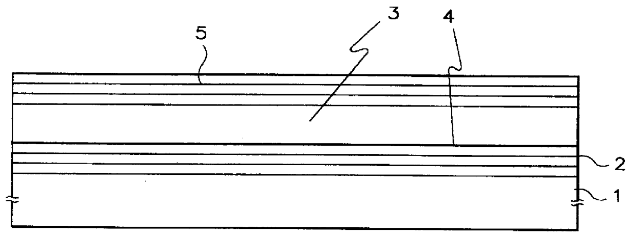
This invention is directed to a method of fabricating a 200-400 nm short-wavelength optoelectronic device from a semiconductor having a 5-6 eV energe band gap, and based on a principle that an electron-hole pair is produced using a highly energetic electron which is injected from a field emission device, and a photon is emitted when the electron recombines with the hole. The optoelectronic device is provided with a quantum well layer and a Bragg diffraction superlattice layer, and the quantum well layer is interposed between the superlattice layer and a light reflection layer underlying the superlattice layer. Electrons and holes are confined in the quantum well layer for a concentrated recombination, as a result of which it is possible to maximally enhance the efficiency in producing electron-hole pairs from the electron beam and concentrate the photons at a single energy level.

El...


PUM


Abstract

Provided with a method of fabricating a 200-250 nm short-wavelength optoelectronic device, which has a combination of an optical device with a plurality of acceleration electrodes and a field emission device with a plurality of acceleration electrodes, from a semiconductor having a 5-6 eV energe band gap, based on a principle that an electron-hole pair is produced using a highly energetic electron which is injected from a field emission device, and short-wavelength photons are emitted when the electron recombines with the hole and confined in a quantum well to emit a light corresponding to the energy level of the quantum well, thereby eliminating the need of using dopants for forming n-p junctions in the semiconductor and achieving high efficiency in terms of energy because highly energetic electrons result in one or more electron-hole pairs.

Description

1. Field of the InventionThe present invention relates to a short-wavelength optoelectronic device having the combination of a field emission device and an optical device, and its fabricating method.2. Description of the Prior ArtShort-wavelength lasers are used in a variety of applications such as optical recording medium for display with enhanced record density, medical appliances, and measuring instruments. In particular, a use of short-wavelength laser makes it possible to enhance the optical record density several scores of times as high as the current density of several giga bytes such that the capacity of data communication device such as multimedia information server can be greatly increased. However, ultraviolet lasers employing He--Cd gas plasma or frequency modulation method are inapplicable to the microelectronics because they are extremely large in volume and very expensive.On the contrary, many studies and developments have been vigorously made on the WBG (Wirde Band G...

Claims


Application Information

Patent Timeline
IPC IPC(8): H01J9/02H01L33/00H01S5/04H01S5/00H01S5/183H01L33/32
CPCH01J9/025H01L33/32H01S3/0959H01S5/0207H01S2304/02H01S5/04H01S5/183H01S2301/173H01S5/0261H01L33/00
Inventor SHIM, KYU HWANCHOI, SUNG WOOBAEK, MUN CHEOLCHO, KYOUNG IKLEE, HAE GWON
Owner ELECTRONICS & TELECOMM RES INST
Why Eureka
Try Eureka