Hybrid organic-inorganic planar optical waveguide device

a planar optical waveguide and organic technology, applied in the direction of optical elements, manufacturing tools, instruments, etc., can solve the problems of long deposition time, high cost of all process steps, and painstaking patterning technology, so as to minimize stress fields and reduce the effect of stress induced polarization

Inactive Publication Date: 2000-11-07
CORNING INC
View PDF9 Cites 123 Cited by
  • Summary
  • Abstract
  • Description
  • Claims
  • Application Information

AI Technical Summary

Benefits of technology

rocess. This is a very significant advantage of the invention.
In combination, a complete planar waveguide structure can be made, or if desired, an overclad layer may be provided on a conventionally etched silicate core waveguide array. The primary advantage that can be realized from this invention is cost. The use of the inventive overclad on conventionally patterned glass waveguide arrays can provide advantages. The low process temperature used avoids any deformation of the waveguide cores, whereas high temperature processing can distort the original waveguide shape. The low temperature and low modulus of the ...

Problems solved by technology

All of the variations on these process steps share an intrinsic high cost.
Deposition times are long and patterning techn...

Method used


Image

  • Hybrid organic-inorganic planar optical waveguide device
  • Hybrid organic-inorganic planar optical waveguide device
  • Hybrid organic-inorganic planar optical waveguide device

Examples


Embodiment Construction

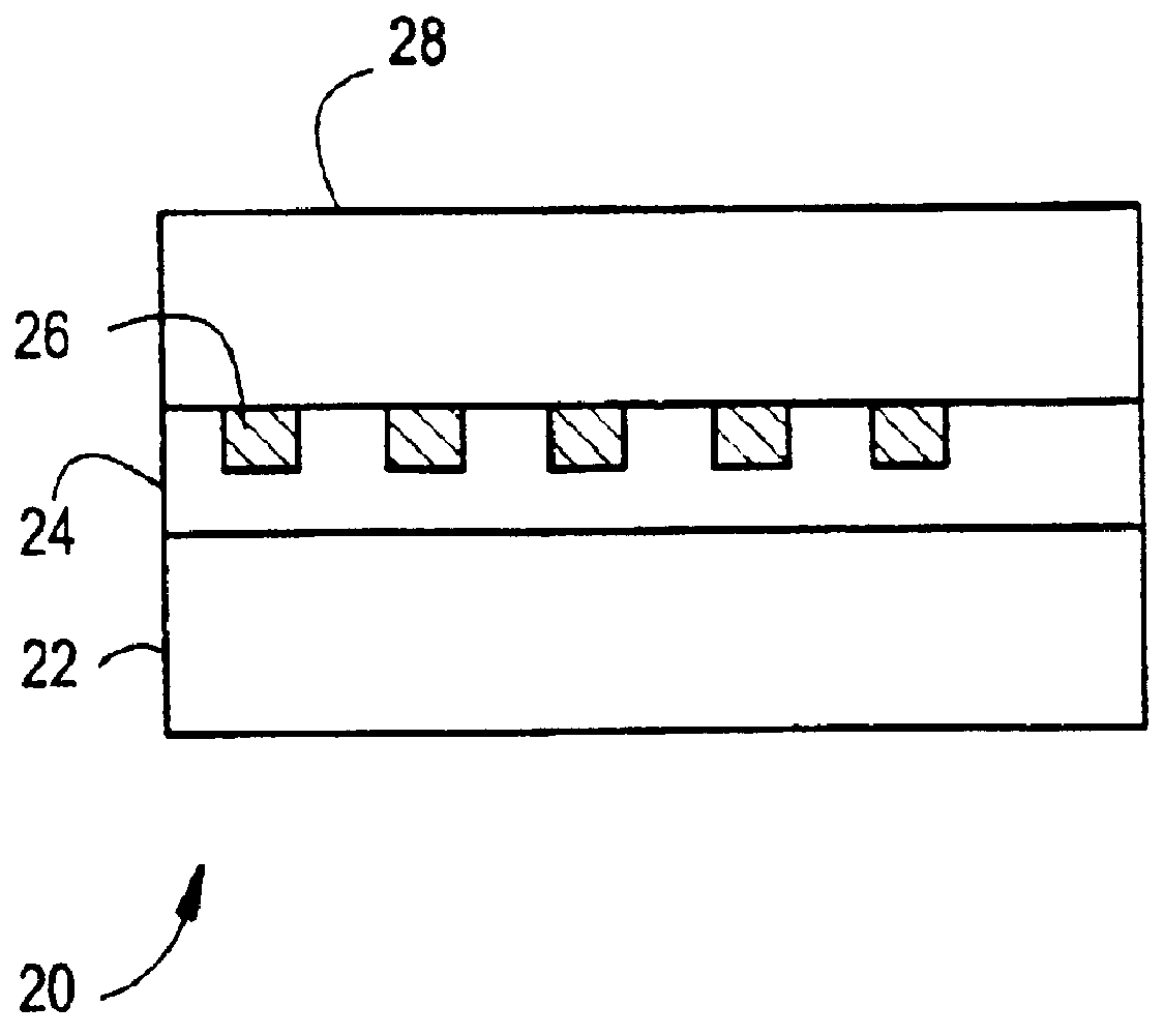
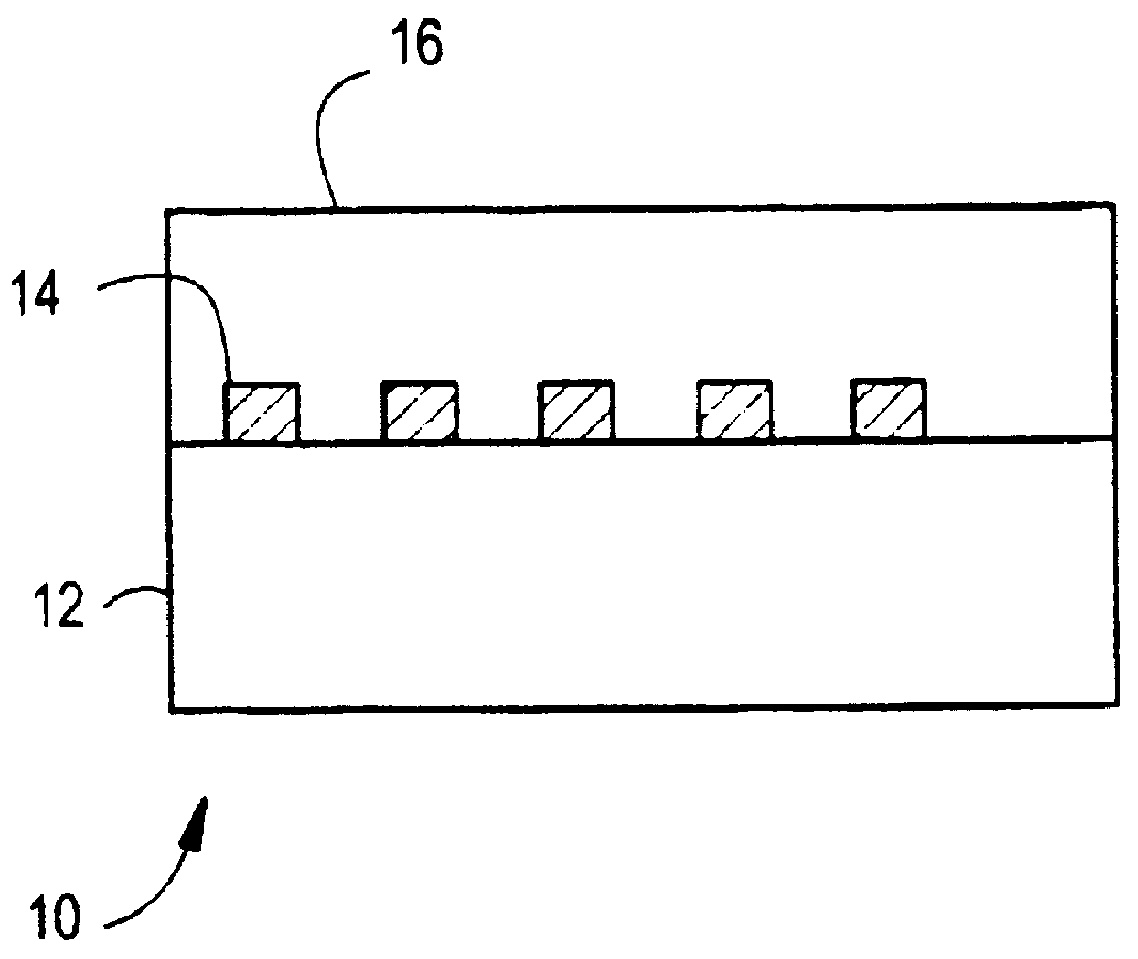
Used to Form Planar Optical Waveguide Devices

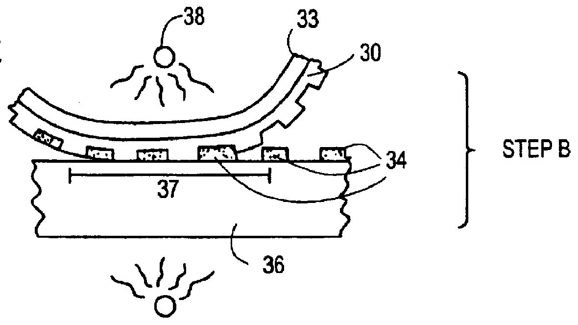
The inventions is further described in connection with the following specific examples.

One suitable material for this invention is invention is a sol-gel based silsesquioxane. The materials is made from a multicomponent mixture of alkyl- and aryalkoxysilanes, and water.

C.1 Synthetic Preparation I

The following describes a process for forming a core or cladding composition starting from a core or cladding composition precursor material.

The preparation is based on a 0.03 moles of silicon formulation with 8 mole % equivalent PDMS (polydimethylsiloxane), 73% MTES (methyltriethoxysilane) and 19% PTES (phenyltriethoxysilane). This will provide a material with an index of refraction of about 1.4565 at 632 nm (clad formulation). The composition for a core index (1.465) is given in {brackets}.

Volumes

HF and PTES are mixed together in a closed nalgene vessel. The mixture is then heated in a 75.degree. C. water bath for 15 to 30 minutes. This step pre...


PUM

PropertyMeasurementUnit
Fractionaaaaaaaaaa
Fractionaaaaaaaaaa
Fractionaaaaaaaaaa

Abstract

PCT No. PCT/US97/22760 Sec. 371 Date Jun. 10, 1999 Sec. 102(e) Date Jun. 10, 1999 PCT Filed Dec. 12, 1997 PCT Pub. No. WO98/26315 PCT Pub. Date Jun. 18, 1999A planar optical device is formed on a substrate (12) and comprising an array of waveguide cores (14) and a cladding layer (16) formed contiguously with the cores. At least one of the array of waveguide cores (14) and the cladding layer (16) is an inorganic-organic hybrid material that comprises an extended matrix containing silicon and oxygen atoms with at least a fraction of the silicon being directly bonded to substituted or unsubstituted hydrocarbon atoms. In accordance with other embodiments of the invention, a method of forming an array of cores comprises the steps of preparing a core composition precursor material; partially hydrolyzing and polymerizing the material; forming an array of waveguide cores under conditions effective to form an inorganic-organic hybrid material that comprises an extended matrix containing silicon and oxygen atoms with at least a fraction of the silicon being directly bonded to substituted or unsubstituted hydrocarbon atoms.

Description

The present invention relates to a planar optical waveguide device in which one of the layers is formed according to a hybrid inorganic-organic material processing method. In particular, one of the layers is an inorganic-organic hybrid material that comprises an extended matrix containing silicon and oxygen atoms in which a fraction of the silicon atoms are directly bonded to substituted or unsubstituted hydrocarbon moieties. The present invention also relates to a method for forming a planar optical waveguide device without the use of a lithographic process. Preferably, the inorganic-organic material comprises a solid material comprised of methyl-siloxane groups, phenyl-siloxane groups, and fluorine which is provided by thermally curing a precursor mixture comprised of polydimethyl-siloxane, methyl trialkoxy silane, phenyl trialkoxy silane, and a structural modifier including a fluorine atom.A typical planar optical waveguide device includes a planar substrate, an array of waveguid...

Claims


Application Information

Patent Timeline
IPC IPC(8): C03B19/12C03C17/34C03C17/00G02B6/132G02B6/13G02B6/122G02B6/138
CPCC03B19/12C03C17/007C03C17/009C03C17/34G02B6/138G02B6/1221G02B6/13G02B6/132C03C2217/40
Inventor DAWES, STEVEN B.JOHNSON, RONALD E.MASCHMEYER, RICHARD O.SHOUP, ROBERT D.
Owner CORNING INC
Why Eureka
Try Eureka