

Multi-junction photovoltaic device with microcrystalline I-layer
a photovoltaic device and microcrystalline technology, applied in the field of photovoltaic elements, can solve the problems of narrow band gap of microcrystalline silicon, low photoelectric conversion efficiency of this photovoltaic element, and low stabilization efficiency of elements described in fischer
- Summary
- Abstract
- Description
- Claims
- Application Information
AI Technical Summary
Benefits of technology
Problems solved by technology
Method used
Image

Examples
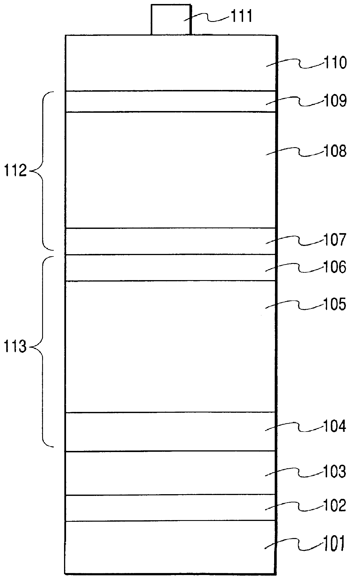
example 2
The present example is different from Example 1 in that in the deposition of the microcrystal SiC-i layer 108, the flow rates of SiH.sub.4 and CH.sub.4, the RF power, and the substrate DC voltage out of the forming conditions were varied with the passage of time, whereby the compositional ratio x of carbon (Si.sub.1-x C.sub.x) in the microcrystal SiC-i layer was varied and whereby the grain diameter and volume percentage of microcrystal Si or microcrystal SiC were varied in the film thickness direction.
The photovoltaic elements of Example 2 were fabricated in the same manner as in Example 1, except for the above point.
The deposition conditions of the microcrystal SiC-i layer 108 were called A at the time of start of deposition, B at the time when the compositional ratio of carbon reached a minimum during deposition, and C at the end of deposition. The deposition conditions were continuously changed between the respective deposition conditions.
After fabrication of the photovoltaic el...
example 3
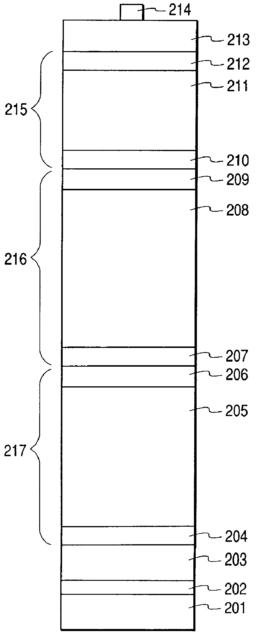
In the present example, the triple type photovoltaic element was fabricated which had three pin junctions stacked as shown in FIG. 2. The photovoltaic element of the present example is characterized in that, when counted from the light incidence side, the first pin junction 215 has the i-type semiconductor layer 211 comprised of microcrystal SiC, the second pin junction 216 has the i-type semiconductor layer 208 comprised of microcrystal Si, and the third pin junction 217 has the i-type semiconductor layer 205 comprised of microcrystal SiGe.
The photovoltaic element of the present example was fabricated according to the following steps, using the forming apparatus by the roll-to-roll method shown in FIGS. 6A and 6B, which was described previously.
(1) Setting of Substrate in the Apparatus of FIGS. 6A and 6B
The substrate was a sheet of belt-like stainless steel (SUS430BA) measuring the length 100 m, the width 30 cm, and the thickness 0.15 mm. The SUS430BA sheet was wound around a feed ...
example 4
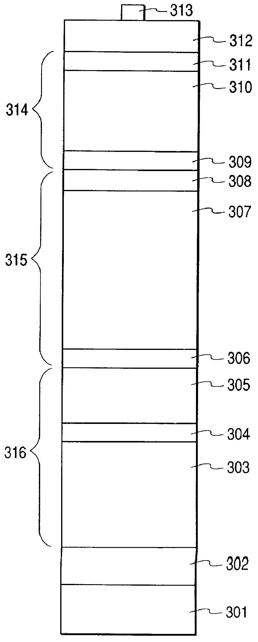
The present example is different from Example 3 in that when forming the i3 layer 211 comprised of microcrystal SiC, the compositional ratio of carbon, and the grain diameter and volume percentage of microcrystals were varied in the film thickness direction as shown in FIGS. 7A to 7C by varying the ratio of flow rates of SiH.sub.4 gas and CH.sub.4 gas, effective microwave power, and effective RF bias power in the transfer direction of the belt-like substrate.
In FIGS. 7A to 7C, A denotes the interface between the n-layer 210 and the i3 layer 211, B the thickness at the minimum compositional ratio of carbon, and C the interface between the i3 layer 211 and the p3 layer 212. The compositional ratios were evaluated by analysis in the depthwise direction by AES and the grain diameters and volume percentages of microcrystals by observation by x-ray diffraction and a TEM.
It was found from FIGS. 7A to 7C that from point A to point B, i.e., from the interface with the n-layer to the thicknes...
PUM
| Property | Measurement | Unit |
|---|---|---|
| grain diameter | aaaaa | aaaaa |
| grain diameter | aaaaa | aaaaa |
| thickness | aaaaa | aaaaa |
Abstract
Description
Claims
Application Information