Transconductance filter control system

a control system and filter technology, applied in gain control, frequency selective two-port networks, continuous tuning, etc., can solve the problems of large silicon wafer or circuit size, large power consumption, and inability to manually adjus

Inactive Publication Date: 2001-01-09
ANALOG DEVICES INC +1
View PDF7 Cites 39 Cited by
  • Summary
  • Abstract
  • Description
  • Claims
  • Application Information

AI Technical Summary

Benefits of technology

It is a further object of this invention to provide such a system which avoids problems associated with clocked feedback loops, such as high power consumption, large silicon wafer or circuit size, complex design criteria, and clock-induced noise coupling.

Problems solved by technology

Since this transconductance gain varies in accordance with several variables, such as temperature variations, process variations (such as transistor doping levels) and production variations (such as transistor channel width, transistor channel length, etc.), a transconductance filter circuit is prone to uncontrollable filter characteristic shifts which severely effect the stability and overall usability of the filter.
However, manual adjustment is not always possible or practical.
However, there are several disadvantages associated with the use of this PLL or DLL as an automatic control circuit for a transconductance filter circuit.
Specifically, these disadvantages include: the additional power required to drive such a PLL or DLL circuit; the additional wafer size (or PC board size) required to construct such a circuit; the complex design criteria and time required to construct such a PLL or DLL circuit; and the undesirable coupling of the PLL / DLL clock signal with the transconductance filter circuit which results in the imposition of PLL / DLL induced noise into the output of the transconductance filter circuit.

Method used


Image

  • Transconductance filter control system
  • Transconductance filter control system
  • Transconductance filter control system

Examples


Embodiment Construction

Other objects, features and advantages will occur to those skilled in the art from the following description of a preferred embodiment and the accompanying drawings, in which:

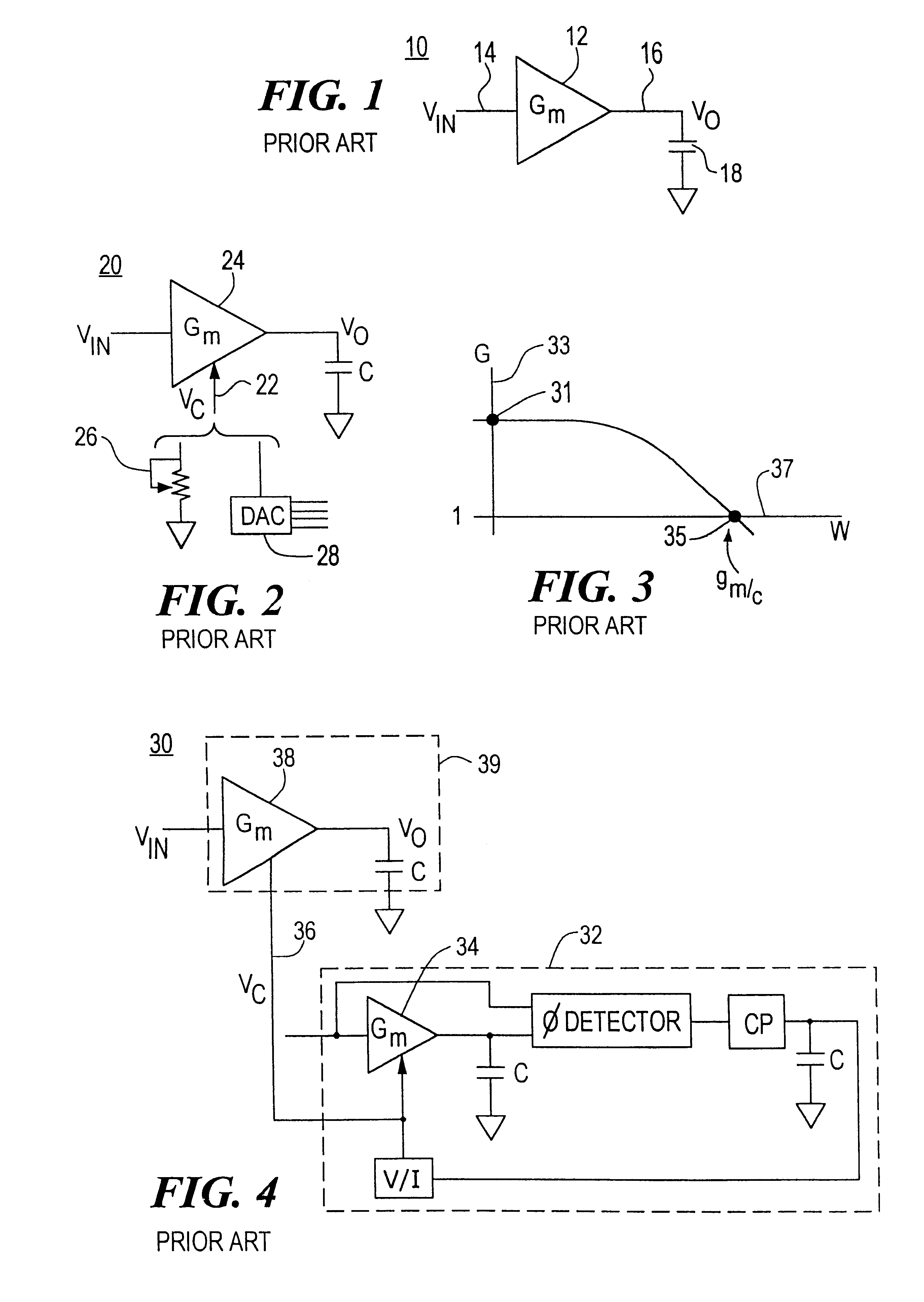
FIG. 1 is a schematic view of a prior art transconductance filter circuit;

FIG. 2 is a schematic view of a prior art transconductance filter circuit incorporating a manual transconductance control circuit;

FIG. 3 is a graph showing the frequency response of a prior art transconductance filter;

FIG. 4 is a schematic view of a prior art transconductance filter circuit incorporating a phase look loop based automatic transconductance control circuit;

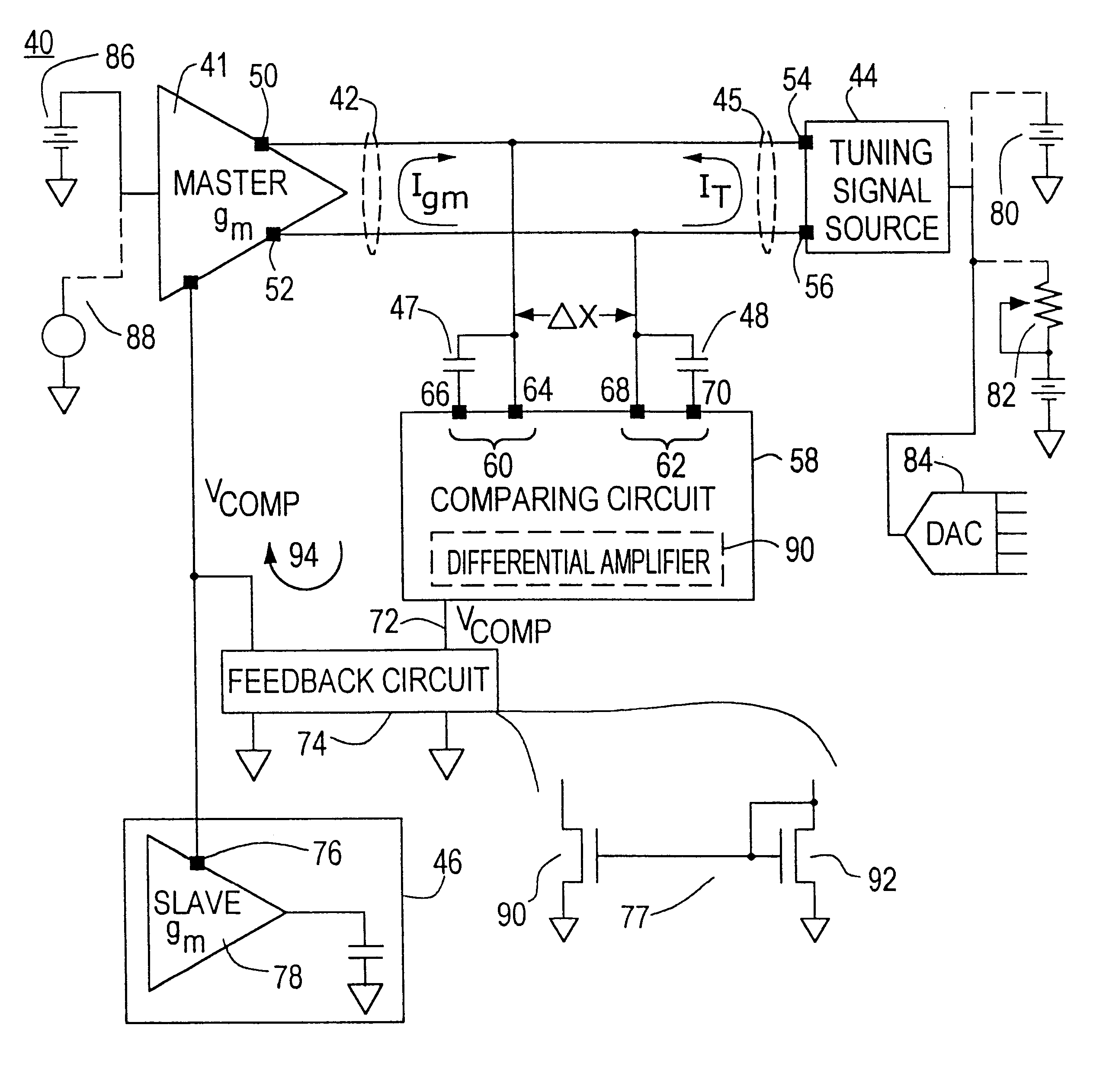
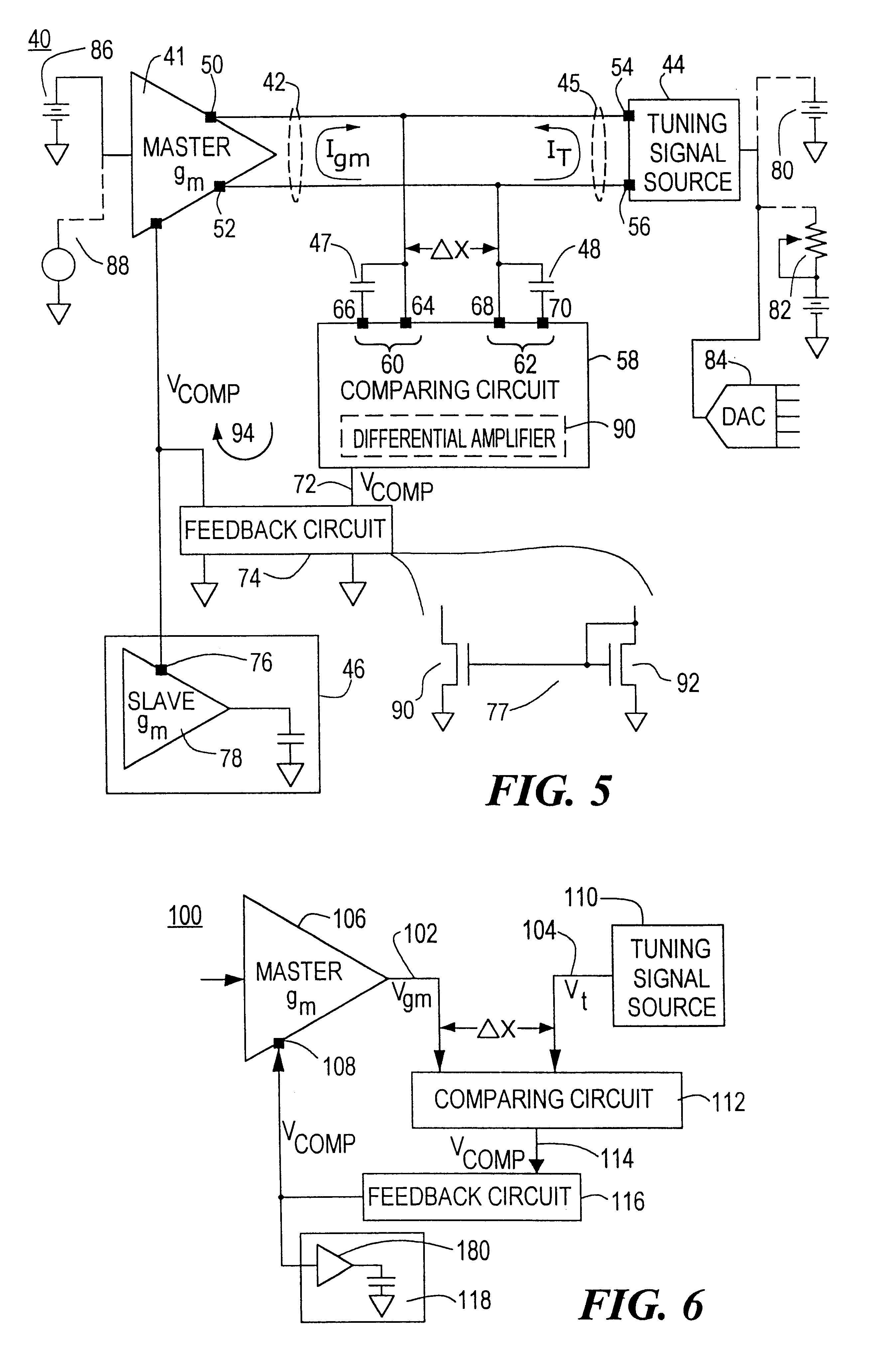
FIG. 5 is a schematic view of the transconductance filter control system of this invention in which the output of the master transconductance amplifier and the tuning signal are currents;

FIG. 6 is a diagrammatic view of another embodiment of the transconductance filter control system of this invention in which the output of the master transconductance amplifier and the tun...


PUM


Abstract

A transconductance filter control system for compensating for drift in transconductance of a slave transconductance amplifier in a continuous time transconductance filter including: a master transconductance amplifier having an output which is a function of its transconductance and a control input for controlling the transconductance of the master transconductance amplifier; a tuning signal source for providing a tuning signal representative of a preselected characteristic of the transconductance filter; a comparing circuit, responsive to any deviation from a predetermined difference between the tuning signal and the output of the master transconductance amplifier, representative of a deviation of the transconductance of the master transconductance amplifier, for providing a compensation signal; and a circuit for applying the compensation signal to the control input of the master transconductance amplifier and to the control input of the slave transconductance amplifier in the transconductance filter to adjust the transconductance of both the master and slave transconductance amplifiers and restore the predetermined difference between the tuning signal and the output of the master transconductance amplifier.

Description

This invention relates to a transconductance filter control system and more specifically to such a filter control system which automatically compensates for variations in transconductance gain.BACKGROUND OF INVENTIONTransconductance filters are often used in electronic circuits to perform various filtering functions. Typically, these filters incorporate a transconductance amplifier which converts a voltage input signal into a controlled current signal, where the controlled current signal produced is equal to the product of the transconductance gain (g.sub.m) of the amplifier and the voltage input signal applied to the amplifier. This controlled current signal is then applied to a capacitor to produce an output voltage. Since the voltage across this capacitor varies in accordance with the rate of the change of the current passing through the capacitor and the current passing through the capacitor varies in accordance with the voltage applied to the transconductance amplifier, a frequ...

Claims


Application Information

Patent Timeline
Patent Type & Authority Patents(United States)
IPC IPC(8): H03H11/04H03J3/00H03J3/04H03H11/00H03H11/54
CPCH03H11/0422H03J3/04H03H11/54
Inventor MCCALL, KEVIN J.SPAULDING, JR., GEORGE R.
Owner ANALOG DEVICES INC
Why Eureka
Try Eureka