
GaAs single crystal substrate and epitaxial wafer using the same

Inactive Publication Date: 2001-01-30
SUMITOMO ELECTRIC IND LTD
View PDF8 Cites 10 Cited by
  • Summary
  • Abstract
  • Description
  • Claims
  • Application Information

AI Technical Summary

Benefits of technology

When the GaAs single crystal substrate in accordance with the present invention is used as a substrate for an epitaxial wafer, generation of slips when the temperature is increased can be suppressed, because of the influence of carbon and boron impurity concentrations and because of the characteristics of lower residual strain and dislocation density attained by thermal hysterisis control. As a result, production yield of the devices can be improved significantly.
Further, as the EL2 concentration is kept low while boron concentration is increased, high resistance is realized. As a result, the breakdown withstanding characteristic can be improved when the devices are fabricated.
In this manner, by controlling concentrations of impurities in the raw material melt and controlling thermal hysterisis after solidification, the GaAs single crystal substrate which meets the characteristics of the present invention can be fabricated.
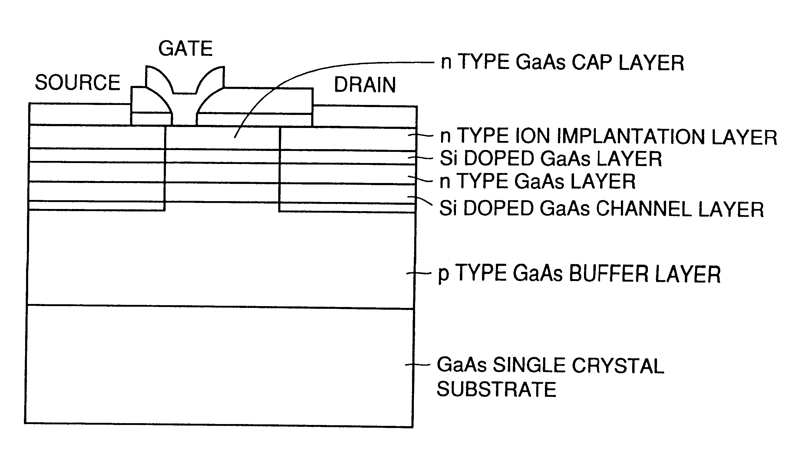
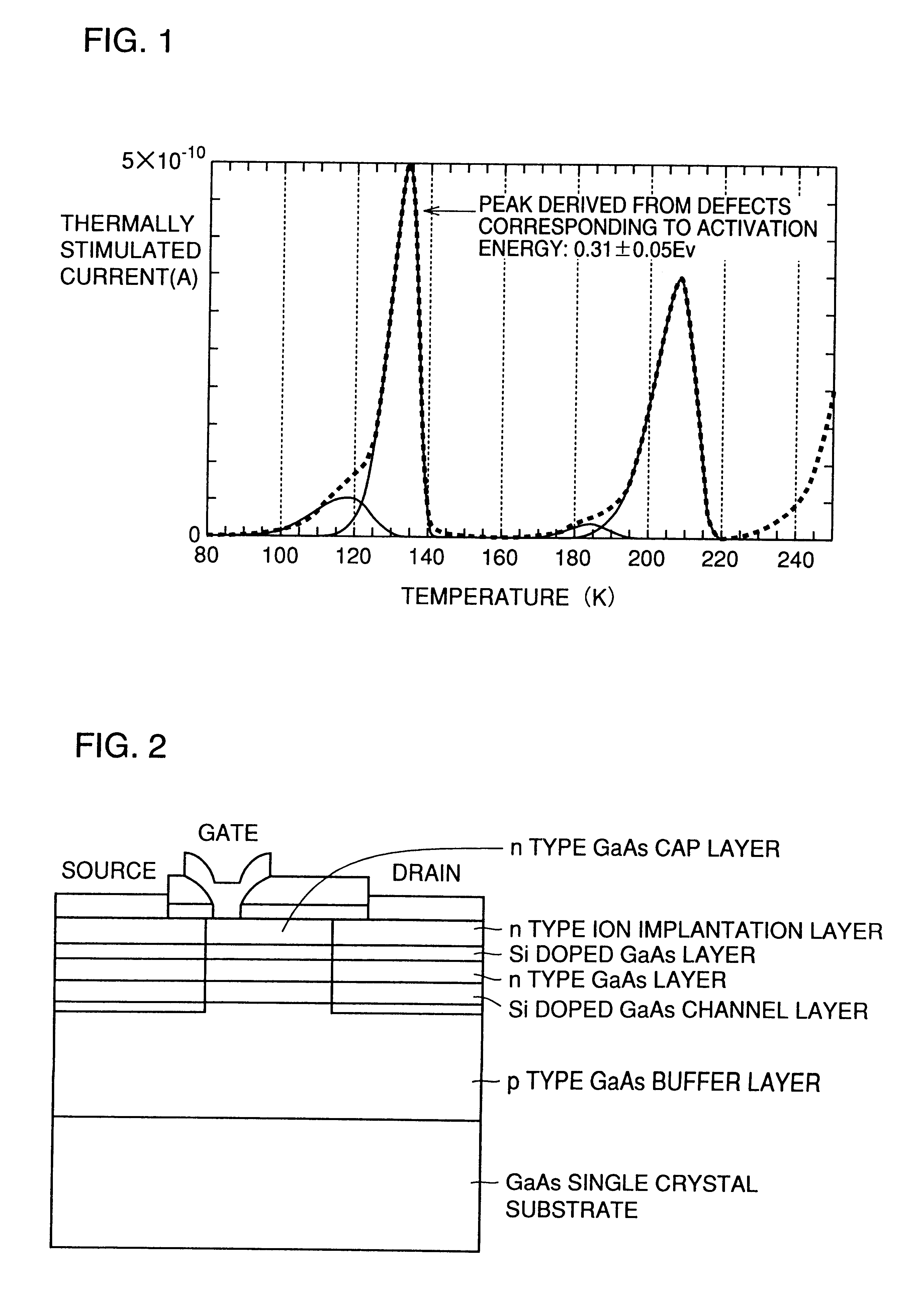
Further, when the GaAs single crystal substrate in accordance with the present invention is used as a substrate for an epitaxial wafer, higher resistance can be attained, as the deep level (activation energy of 0.31.+-.0.05 eV) detected by the thermally stimulated current method is high. As a result, the breakdown withstanding characteristic at the time of fabricating devices can further be improved.

Problems solved by technology

The conventional single crystal substrate, however, generally has low carbon concentration and therefore it cannot withstand thermal stress-strain when the temperature is increased to form the actual epitaxial layer, so that steps, which are referred to as slips, result on the substrate surface.
When devices are fabricated on the steps, desired device characteristics cannot be attained, and hence production yield is significantly degraded.

Method used


Image

  • GaAs single crystal substrate and epitaxial wafer using the same
  • GaAs single crystal substrate and epitaxial wafer using the same

Examples


Embodiment Construction

Samples of GaAs single crystal having the diameter of 100 mm and the length of straight body of 100 mm were grown through the VB method.

Other than raw material GaAs, carbon and boron were added with the amounts to be added changed variously on the order of ppm, and melted together with the raw material GaAs, and a crystal was grown in thermal environment having temperature gradient of 2 to 10.degree. C. / cm. After the crystal was grown, the samples were cooled at a rate of 10 to 100.degree. C. / hour. Thereafter, the crystal samples were subjected to heat treatment at the temperature range of 100 to 1000.degree. C. in a heat treatment furnace.

Characteristics of the crystal samples obtained in this manner are as shown in Tables 1 to 3.

Carbon concentration and EL2 concentration were calculated based on absorption of light at a prescribed wavelength. Impurity concentration other than carbon was evaluated by glow discharge mass spectrometry (GDMS), the resistivity was evaluated by Hall eff...


PUM

PropertyMeasurementUnit
Diameteraaaaaaaaaa
Breakdown voltageaaaaaaaaaa

Abstract

A GaAs single crystal substrate and an epitaxial wafer using the same suppress the generation of slips during growth of the epitaxial layer, and improve the breakdown withstanding characteristic of devices fabricated on such substrates. The GaAs single crystal substrate has a mean dislocation density in plane of at most 2x104 cm-2, a carbon concentration of 2.5 to 20.0x1015 cm-3, a boron concentration of 2.0 to 20.0x1016 cm-3, an impurity concentration other than carbon and boron of at most 1x1017 cm-3, an EL2 concentration of 5.0 to 10.0x1015 cm-3, resistivity of 1.0 to 5.0x10⁸ OMEGA.cm and a mean residual strain measured by photoelastic analysis of at most 1.0x10⁻⁵.

Description

1. Field of the InventionThe present invention relates to a GaAs single crystal substrate and an epitaxial wafer using the same. More specifically, the present invention relates to a GaAs (gallium arsenide) single crystal substrate used for an integrated circuit and a microwave element, and to an epitaxial wafer using the same.2. Description of the Background ArtSemi-insulating GaAs crystal has been conventionally fabricated through a manufacturing method such as Liquid Encapsulated Czochralski method (LEC method) and Vertical Bridgeman method (VB method).It has been possible to control dislocation density of the GaAs single crystal substrate within the range of 1000 to 100000 cm.sup.-2, by adjusting temperature gradient and cooling rate at the time of growth.Carbon concentration and EL2 concentration of the GaAs single crystal substrate have been controlled by adjusting impurity concentration of a solution, ratio of Ga with respect to As and thermal hysterisis after solidification....

Claims


Application Information

Patent Timeline
IPC IPC(8): C30B11/00H01L21/02H01L21/205H01L21/20C30B29/42
CPCC30B11/00H01L21/02395H01L21/02463H01L21/0262H01L21/02546C30B29/42Y10T428/265
Inventor HAGI, YOSHIAKINAKAI, RYUSUKE
Owner SUMITOMO ELECTRIC IND LTD
Learn More