

Reusable modules for complex integrated circuit devices
- Summary
- Abstract
- Description
- Claims
- Application Information
AI Technical Summary
Benefits of technology
Problems solved by technology
Method used
Image

Examples
Embodiment Construction
A. IC Device Design
1. Overview of the Design Process
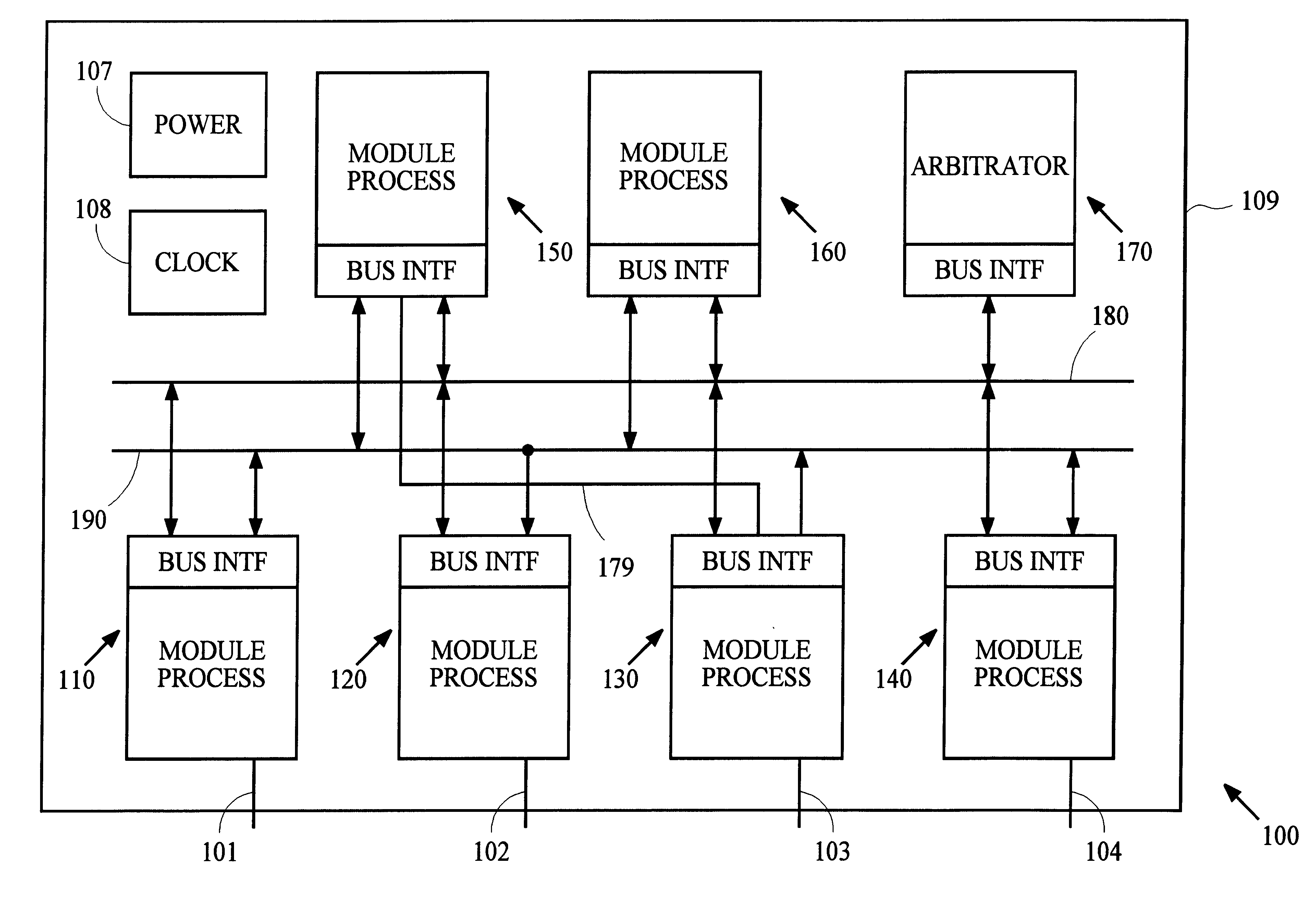
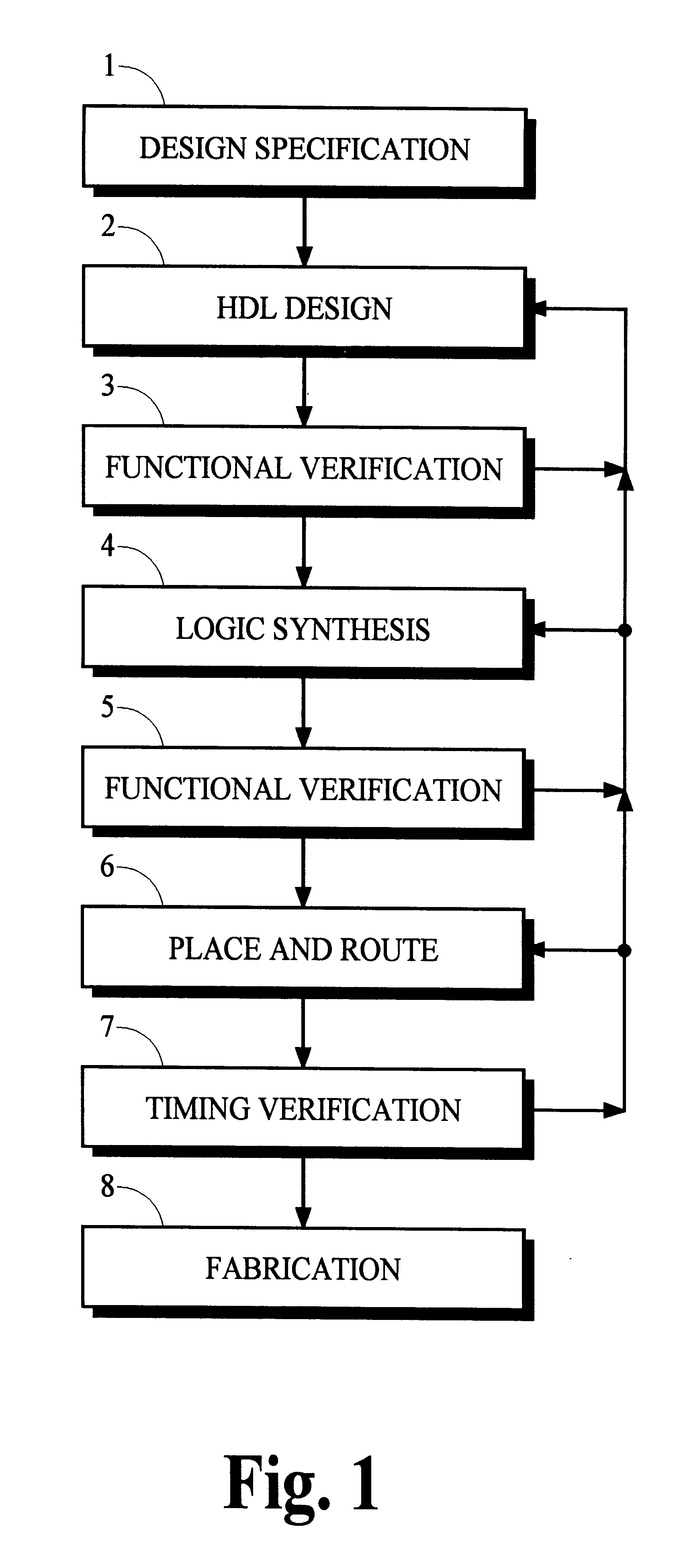
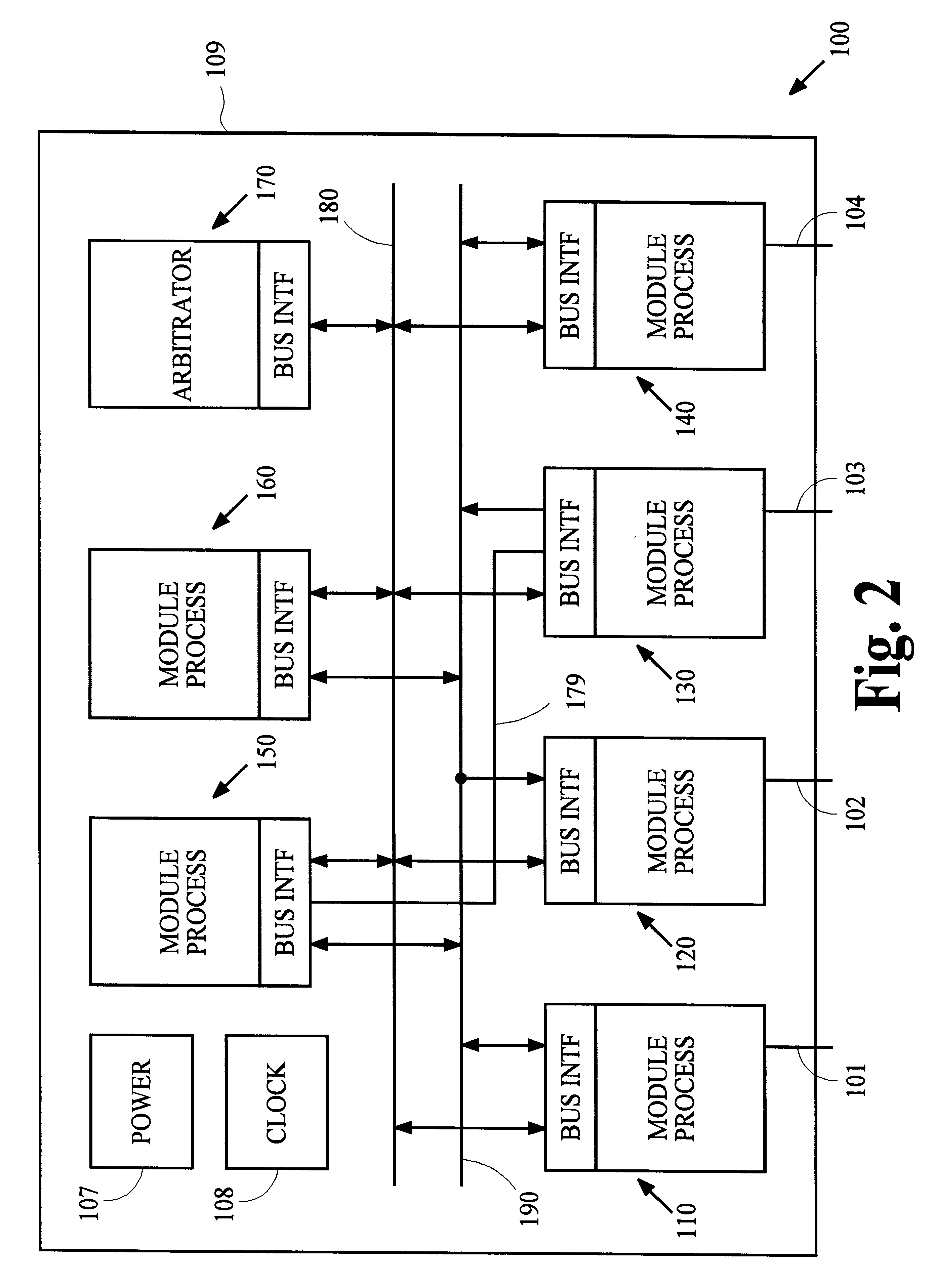
FIG. 1 is a high-level flow diagram of major activities in one process for designing and fabricating an integrated circuit (IC) device. Although the following description omits many details in this process, it provides sufficient information for understanding how the present invention may be applied in such processes.
In step 1, designers develop a specification for the desired IC device that includes items such as the functions to be performed, timing constraints, operating temperature range, and maximum size of the die or substrate on which the IC is to be fabricated.
In step 2, using a hardware description language (HDL) such as Verilog HDL or VHDL, designers can express the IC device in functional terms that are more or less independent of device implementation details. Many HDL can also be used to specify test signals or test vectors to test the HDL design. The HDL is generally recorded on a Machine readable medium such as magne...
PUM
 Abstract
Description
Claims
Application Information