Organic electroluminescent light emitting devices

a technology of electroluminescent light and electroluminescent light, which is applied in the direction of discharge tube/lamp details, discharge tube luminescnet screens, other domestic articles, etc., can solve the problems of poor adhesion of the cathode produced by such a evaporation process using resistance heating to the interface between the cathode and the organic layer, and the aforesaid stabilizing metals, too, are limited

Inactive Publication Date: 2001-04-10
TDK CORPARATION
View PDF5 Cites 42 Cited by
  • Summary
  • Abstract
  • Description
  • Claims
  • Application Information

AI Technical Summary

Problems solved by technology

The reason is that the production process for organic EL devices relies mainly upon evaporation making use of resistance heating, and so the evaporation source used therewith is as a matter of course limited to one having a high vapor pressure at low temperatures.
A cathode produced by such an evaporation process making use of resistance heating is poor in its adhesion to the interface between the cathode and the organic layer.
It is thus believed that the aforesaid stabilizing metals, too, are limited from the standpoint of vapor pressure.
Furthermore, the organic EL element set forth therein fails to solve the aforesaid problem because the constituting films are all formed by evaporation.
However, since the sodium and / or potassium elements are extremely reactive and, hence, unstable materials, it is preferable to mix them with relatively stable other metal for stabilization.
Preferably, a large device such as a display device is interconnected with aluminum or other metal because the resistance of an ITO or other anode is increased, resulting in a voltage drop.
The use of a thin film having a crystal grain diameter exceeding 0.1 .mu.m results in non-uniform light emission.
To avoid this, it is required to increase the driving voltage of the device; however, there is a striking drop of charge injection efficiency.

Method used


Image

  • Organic electroluminescent light emitting devices
  • Organic electroluminescent light emitting devices

Examples


example 1

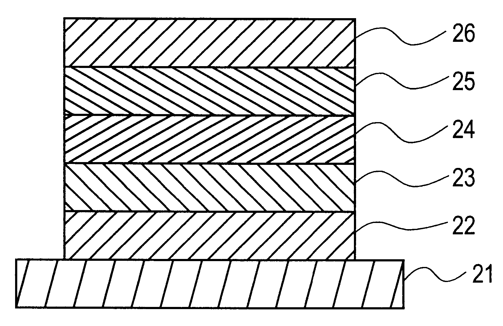
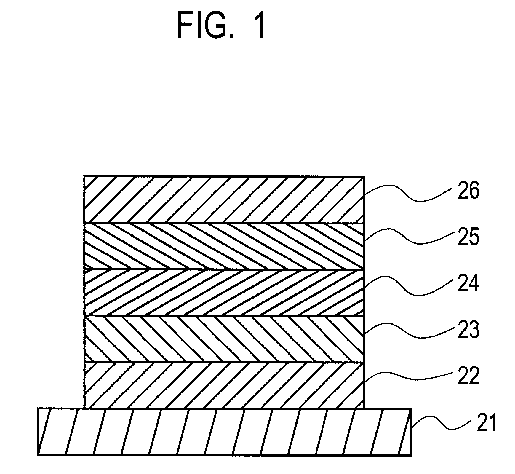
A glass substrate having a 200 nm-thick patterned ITO transparent electrode prepared by a sputtering process was ultrasonically washed with neutral detergent, acetone, and ethanol, and then pulled up from boiling ethanol, followed by drying. This transparent electrode was cleaned on its surface with UV / O.sub.3, after which the substrate was fixed to a substrate holder in a vacuum evaporation system, which was evacuated to a vacuum of 1.times.10.sup.-4 Pa or lower.

While the vacuum was maintained, N,N'-diphenyl-N,N'-m-tolyl-4,4'-diamino-1,1'-biphenyl (TPD) was evaporated at a deposition rate of 0.2 nm / sec. to a thickness of 55 nm to form a hole injecting and transporting layer.

With the vacuum still kept, Alq.sup.3 or tris(8-quinolinolato) aluminum was evaporated at a deposition rate of 0.2 nm / sec. to a thickness of 50 nm to form a light emitting and electron injecting / transporting layer.

With the vacuum still kept, this EL device structure substrate was then transferred from the vacuum...

example 2

An organic EL device was prepared by forming a cathode of 200 nm in thickness as in Example 1. However, the binary sputtering targets used were an Na.Ni target and an Al.Ta target (Ta: 2 at %), and the input power was changed with time from DC 100 to 0 W for the Na.Ni target, and from DC 0 to 500 W for the Al.Ta target.

Observation of the composition of the formed cathode film showed that much Na is present on the interface at which the cathode film is contiguous to the organic layer, with the concentration of Na decreasing gradually in the thickness-wise direction. Here, let Co represent the concentration of Na across a sectional portion of the cathode extending from the interface between the organic layer and the side of the cathode not opposite thereto to the position corresponding to one-third of the cathode thickness, and Ci denote the concentration of Na across a sectional portion of the cathode extending from the interface between the organic layer and the cathode to the posit...

example 3

An organic EL device was obtained as in Example 1, using Na.Ni, and Al.Ta targets as in Example 1. In this example, however, the Al.Ta target was used to laminate an Al.Ta thin film of 150 nm in thickness laminated on a 50 nm thick cathode formed using the Na.Ni target as in Example 1.

This organic EL device was estimated as in Example 1. As a result, it was found that the initial driving voltage drops to 8.5 V, and the half-life of light emission increases to 1,000 hours. The results are shown in Table 1.


PUM

PropertyMeasurementUnit
voltageaaaaaaaaaa
thicknessaaaaaaaaaa
thicknessaaaaaaaaaa

Abstract

An organic EL device comprises a film form of cathode prepared by a sputtering technique, and formed of an alloy of sodium and / or potassium. This cathode is improved in terms of its adhesion to the interface between the cathode and an organic layer and electron injection efficiency, resulting in light emission property improvements. In addition, this cathode causes less damage to the organic layer, is effective for prevention of occurrence of dark spots, and suffers from little or no degradation of performance.

Description

The present invention relates generally to an organic electroluminescent light emitting device (which will hereinafter be often called an organic EL device for short) using an organic compound, and more particularly to an cathode for feeding electrons to a light emitting layer.BACKGROUND TECHNIQUEIn recent years, organic EL devices have been under intensive investigation. One such organic EL device basically includes a transparent electrode (anode) of tin-doped indium oxide (ITO), etc. A thin film is formed on the transparent electrode by evaporating a hole transporting material such as tetraphenyldiamine (TPD). A light emitting layer of a fluorescent material such as an aluminum quinolinol complex (Alq.sup.3) is deposited on the hole transporting thin film. An electrode (cathode) is formed thereon from a metal having a low work function such as magnesium or Mg. This organic EL device attracts attentions because it can achieve a very high luminance ranging from several hundreds to t...

Claims


Application Information

Patent Timeline
Patent Type & Authority Patents(United States)
IPC IPC(8): H01L51/52H01L51/50H05B33/10B32B7/02H05B33/12H05B33/22H05B33/26
CPCH01L51/5221Y10S428/917H10K50/826
Inventor MORI, MASAMI
Owner TDK CORPARATION
Why Eureka
Try Eureka